

Wavelength converting element and method of manufacturing thereof
a technology of converting elements and waveguides, applied in the direction of optical waveguide light guides, light demodulation, instruments, etc., can solve the problems of poor efficiency of joining a semiconductor laser, poor efficiency of joining a te mode, poor waveguide converting efficiency, etc., and achieve the effect of facilitating exposure work and high accuracy patterning
- Summary
- Abstract
- Description
- Claims
- Application Information
AI Technical Summary
Benefits of technology
Problems solved by technology
Method used
Image

Examples
Embodiment Construction
[0036] An embodiment of the present invention will be described in detail hereinafter with reference to the figures.
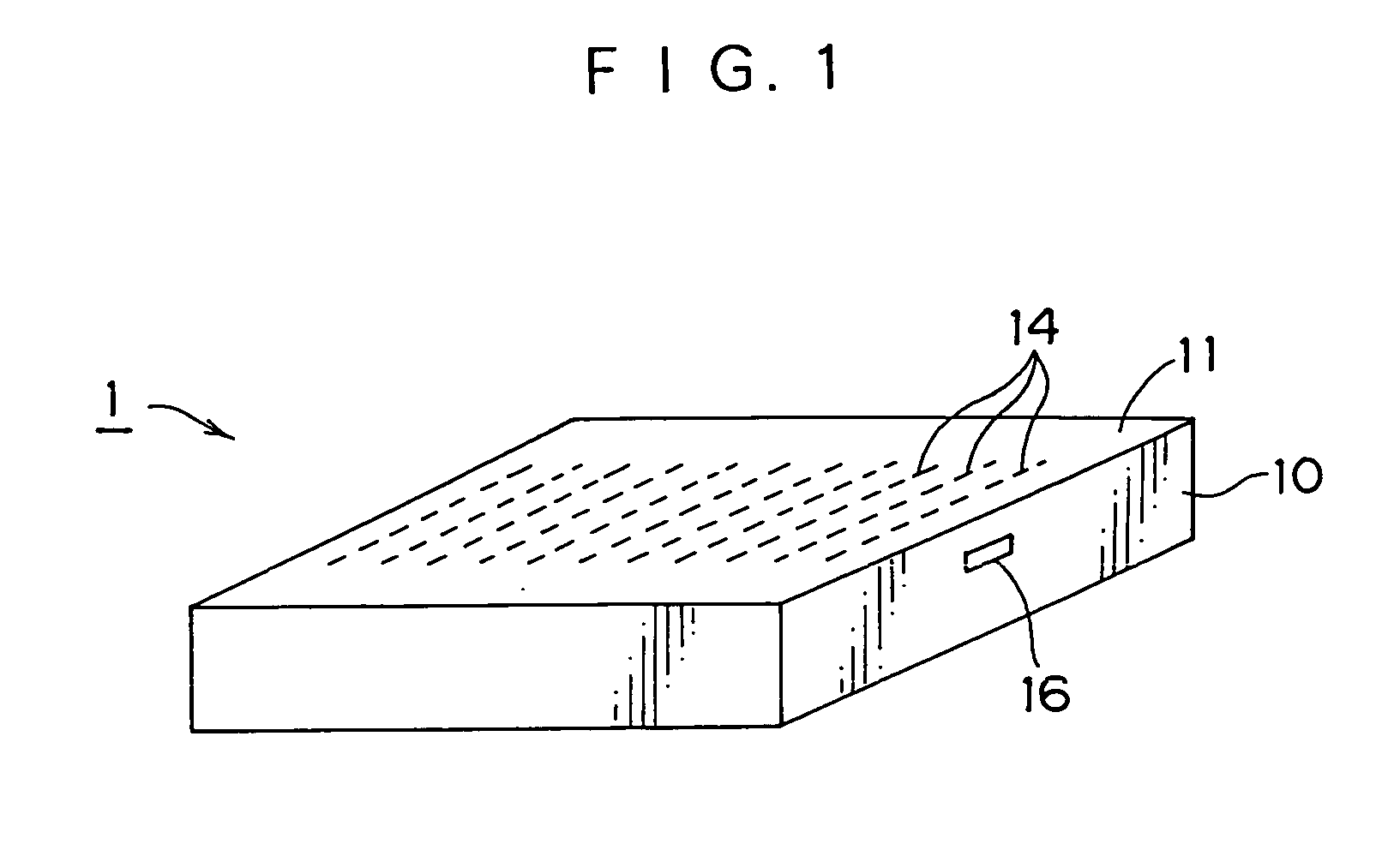
[0037] As shown in FIG. 1, a wavelength converting element 1 relating to the embodiment of the present invention has a plurality of inverted domains 14 which are formed at predetermined intervals at the interior of an optical crystal substrate 10, and a waveguide 16 formed in a direction orthogonal to the respective inverted domains 14.
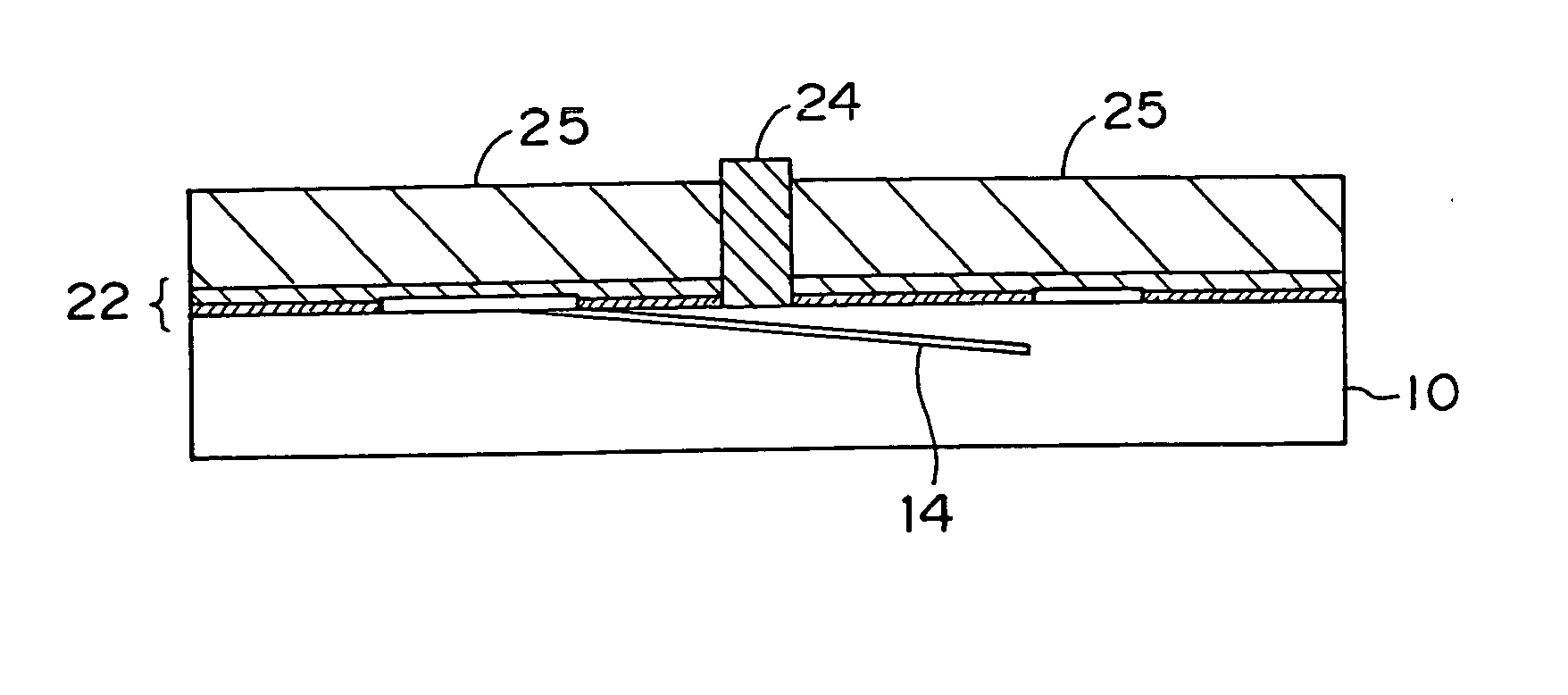
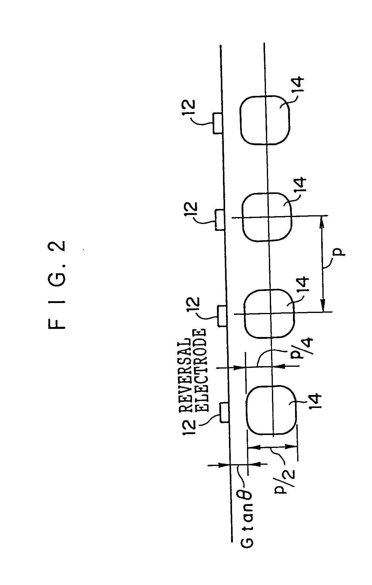
[0038]FIG. 2 is a sectional view of the wavelength converting element 1 shown in FIG. 1, as viewed from the Y axis direction. Comb-shaped reversal electrodes 12 are formed at a main surface 11 of the optical crystal substrate 10. A pitch p between the respective reversal electrodes 12 can be computed from the phase matching wavelength of the second harmonic and the fundamental wave. When the pitch p is determined, the size of the region which optimizes the efficiency of the inverted domains 14 is determined. Usually, the size of the re...
PUM
| Property | Measurement | Unit |
|---|---|---|
| voltage | aaaaa | aaaaa |
| distance | aaaaa | aaaaa |
| transverse width | aaaaa | aaaaa |
Abstract
Description
Claims
Application Information