Non-volatile memory devices and method for forming the same

a memory device and non-volatile technology, applied in nanoinformatics, vehicle sub-unit features, transportation and packaging, etc., can solve the problems of inability to ensure device reliability, degraded data retention characteristics of flash memory devices, and restricted thickness of tunnel oxide layers, so as to prevent etch damage of semiconductor fins and tunnel oxide layers

Active Publication Date: 2005-10-13
SAMSUNG ELECTRONICS CO LTD
View PDF1 Cites 129 Cited by
  • Summary
  • Abstract
  • Description
  • Claims
  • Application Information

AI Technical Summary

Benefits of technology

[0031] According to the above method, a photolithographic process need not be applied to the gate electr...

Problems solved by technology

Accordingly, such restriction to the thickness of the tunnel oxide layer serves as an obstacle to achieve a high integration density.
If the tunneling oxide layer 12 is attacked deeply, a data retention characteristic of the flash memory device is ...

Method used


Image

  • Non-volatile memory devices and method for forming the same
  • Non-volatile memory devices and method for forming the same
  • Non-volatile memory devices and method for forming the same

Examples


Embodiment Construction

[0057] Formation of a nonvolatile memory device having a double gate structure in accordance with the invention will now be described.

[0058] A method for forming a nonvolatile memory device having a double gate structure will be described with reference to FIG. 2, FIGS. 3A through 5A, FIGS. 3B through 5B, FIG. 6, FIGS. 7A through 8A, FIGS. 7B through 8B, FIG. 9, FIG. 10A through 12A and FIGS. 10B through 12B.

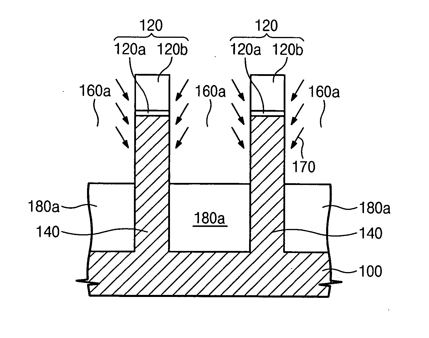
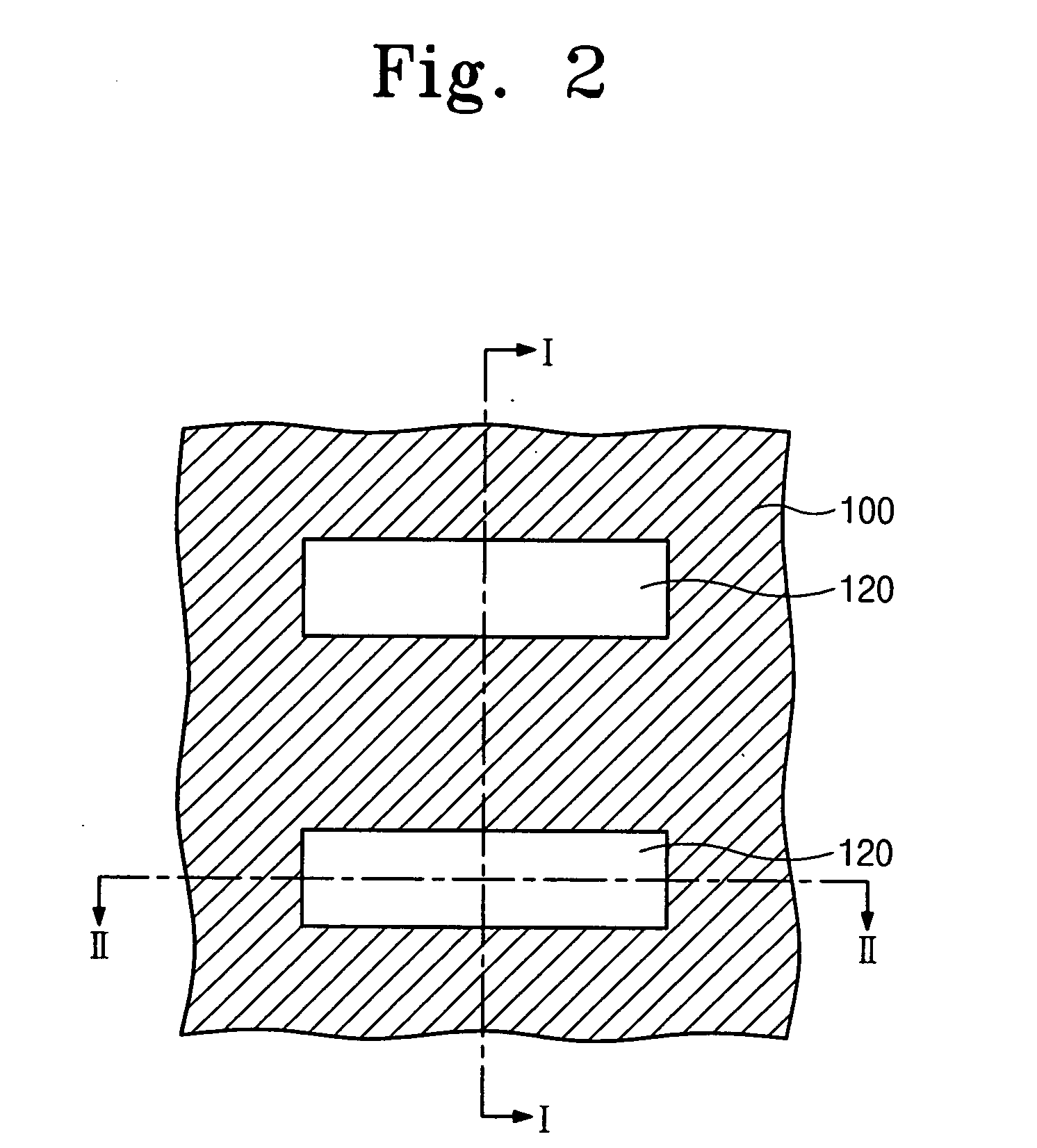
[0059]FIG. 2 is a top plan view of a semiconductor substrate, illustrating a portion of semiconductor substrate including a capping layer pattern for a device isolating layer. FIGS. 3A, 4A and 5A are cross-sectional views of a semiconductor substrate in main fabrication steps of device isolating process, taken along a line I-I of FIG. 2. FIGS. 3B, 4B and 5B are cross-sectional views corresponding to FIGS. 3A, 4A and 5A, respectively, taken along a line II-II in FIG. 2.

[0060] First, referring to FIGS. 2, 3A and 3B, a capping pattern 120 is formed on a semiconductor substrate 1...


PUM


Abstract

According to a nonvolatile memory device having a multi gate structure and a method for forming the same of the present invention, a gate electrode is formed using a damascene process. Therefore, a charge storage layer, a tunneling insulating layer, a blocking insulating layer and a gate electrode layer are not attacked from etching in a process for forming the gate electrode, thereby forming a nonvolatile memory device having good reliability.

Description

CROSS-REFERENCE TO RELATED APPLICATIONS [0001] This U.S. non-provisional patent application claims priority under 35 U.S.C. § 119 of Korean Patent Application 2004-0025095 filed on Apr. 12, 2004, the entire contents of which are hereby incorporated by reference.BACKGROUND OF THE INVENTION [0002] The present invention relates to memory devices and methods for forming the same, and more specifically to non-volatile memory devices and methods for forming the same. [0003] The flash memory device is an electrically programmable non-volatile memory device capable of programming in units of pages or multi-bits and erasing in units of blocks or sectors, thereby having excellent characteristics in respect of speed. The flash memory may be used in various devices such as a digital cellular phone, a digital camera, a LAN-switch, a PC card of a notebook computer, a digital set-top_box, a built-in controller, etc. [0004] As well known, the flash memory device comprises a source / drain, a tunnelin...

Claims


Application Information

Patent Timeline
IPC IPC(8): H01L21/336H01L21/8242H01L21/8246H01L21/8247H01L21/84H01L27/115H01L27/12H01L29/786
CPCB82Y10/00H01L29/78645H01L27/115H01L27/11521H01L27/11568H01L27/1203H01L29/42392H01L29/66545H01L29/66795H01L29/66825H01L29/66833H01L29/785H01L29/7851H01L29/7854H01L21/84H10B43/30H10B69/00H10B41/30B62D15/0205B60Y2410/102B60Y2410/10B60Y2400/70
Inventor OH, CHANG-WOOPARK, DONG-GUNKIM, DONG-WONLEE, YONG-KYU
Owner SAMSUNG ELECTRONICS CO LTD
Why Eureka
Try Eureka