Semiconductor device and method of manufacturing thereof

Active Publication Date: 2005-10-27
DENSO CORP
View PDF11 Cites 36 Cited by
  • Summary
  • Abstract
  • Description
  • Claims
  • Application Information

AI Technical Summary

Benefits of technology

[0020] Thus, the second silicon oxide film is made of the two-layered structure films of the thermal oxide film and the CVD oxide film. Moreover, the total thickness of the two-layered structure films is set to 4 nm or more. It is, therefore, possible to prevent the Vth to an extent of no practical problem from being lowered due to the charge trap phenomenon, and to prevent the Vth from fluctuating due to the enlargement of the bird's beak length by the second silicon oxide film. It is, therefore, possible to prevent the element from being broken by the conc

Problems solved by technology

These tests have revealed such a problem that the threshold value fluctuated to the minus side with the time la

Method used


Image

  • Semiconductor device and method of manufacturing thereof
  • Semiconductor device and method of manufacturing thereof
  • Semiconductor device and method of manufacturing thereof

Examples


Example

[0044] (First Embodiment)

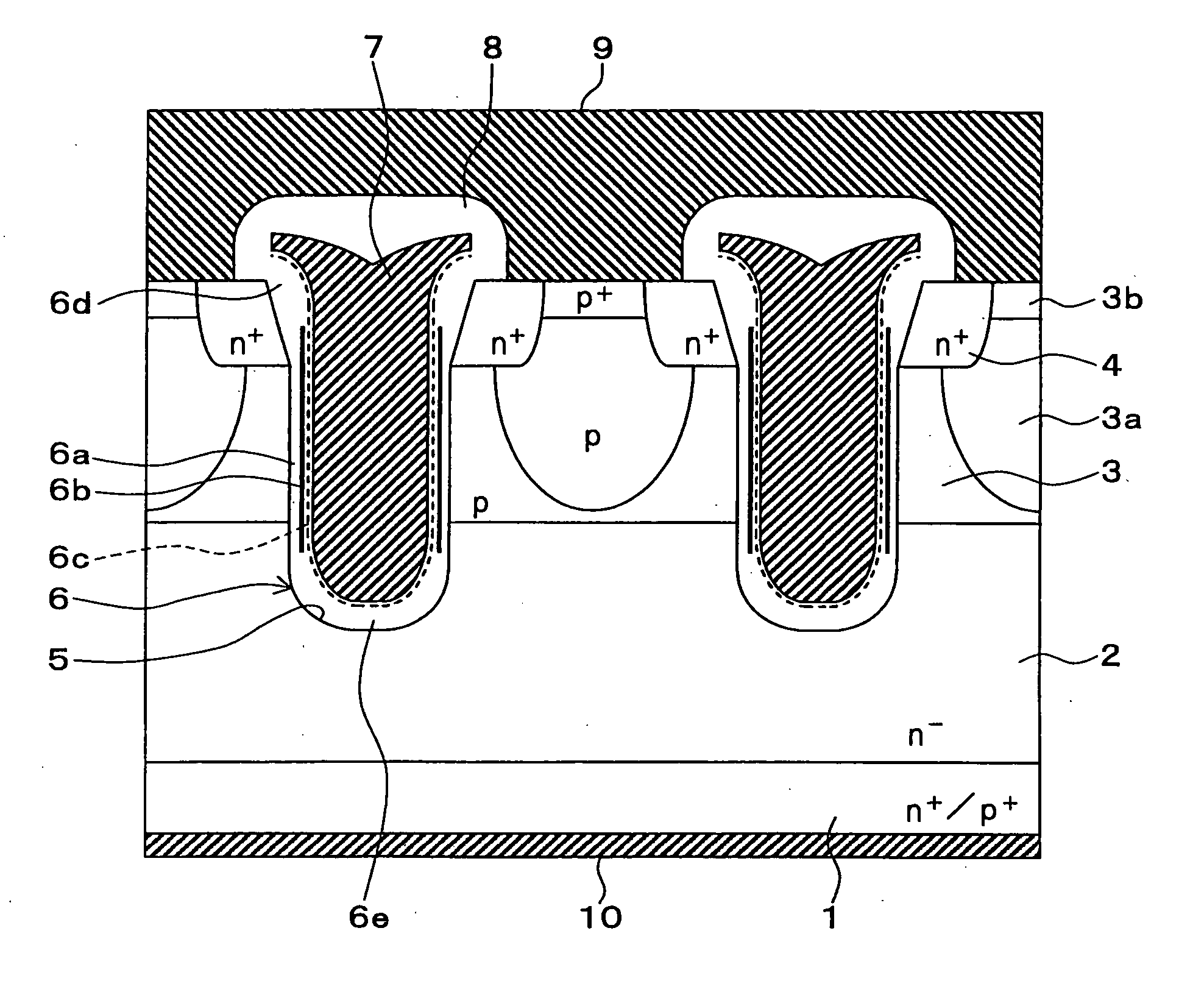
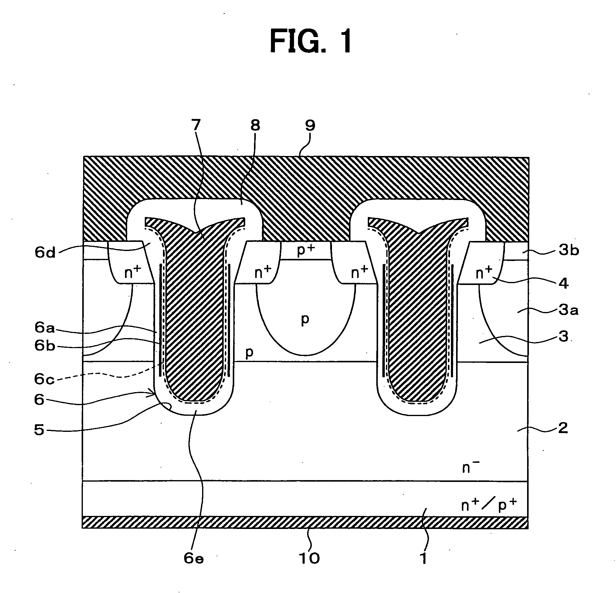
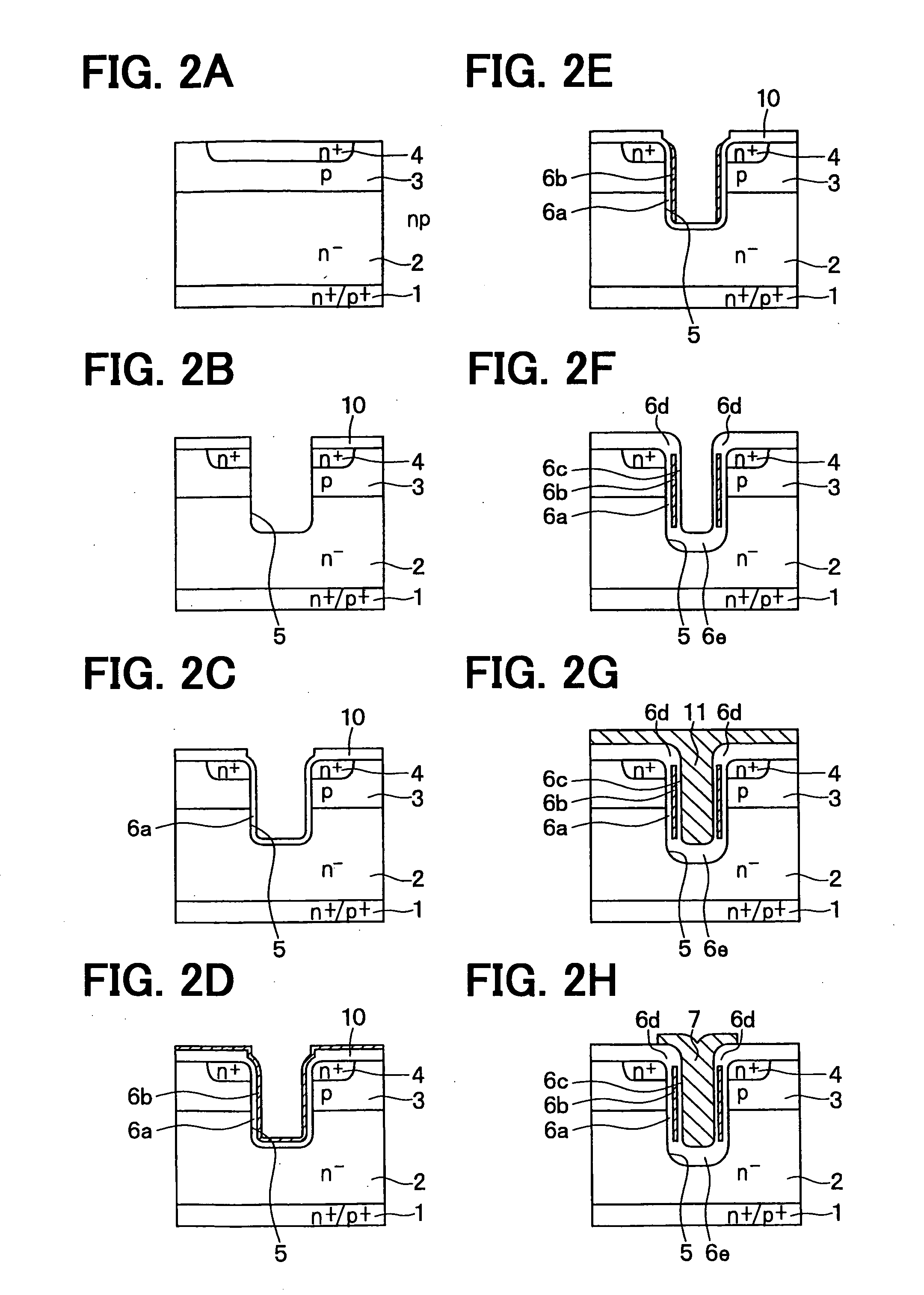
[0045]FIG. 1 shows a sectional structure of a semiconductor device according to one embodiment of the present invention. This semiconductor device is made to include transistors having a trench gate structure such as a power MOSFET, IGBT or the like. However, the present device will be described on the case, in which the transistors are n-channel type elements.

[0046] In FIG. 1, there is formed over an n+-type or p+-type silicon substrate 1 an n−-type drift layer 2, over which is formed a p-type base area 3 for setting a channel area. At the central portion in this p-type base area 3, there is formed a p-type body layer 3a, on the surface portion of which is formed a p+-type contact area 3b.

[0047] Moreover, an n+-type source area 4 is formed in the surface layer portion of the p-type base area 3, and these silicon substrate 1, n−-type drift layer 2, p-type base area 3 and n+-type source area 4 configure the semiconductor substrate. In this semiconductor su...

Example

[0076] (Second Embodiment)

[0077] The foregoing first embodiment has been described on the case, in which the trench-gate type transistor is of the n-channel type element, but the present embodiment will be described on the case, in which the transistor is of the p-channel type element. Here, the structure, in which the transistor is of a p-channel type element, is similar to that of the section shown in FIG. 1, and the conduction types of the individual portions are just reversed, so that the description on the structure is omitted.

[0078] As described above, the case, in which the transistor is the n-channel type element, and the case, in which the same is the p-channel type element, have basically similar structures. Therefore, a similar discussion can be made on the thickness of the silicon oxide film 6c. In the case of the p-channel type element, more specifically, the examination results of the relations between the thickness of the silicon oxide film 6c and the variation ΔVth...

Example

[0085] (Third Embodiment)

[0086] In the foregoing first embodiment, the silicon oxide film 6c is formed at the step shown in FIG. 2F, by performing the step of forming the CVD oxide film after the step of forming the thermal oxide film on the surface of the silicon nitride film 6b. However, these steps can also be reversed. Specifically, the silicon oxide film 6c may be formed by performing the step of forming the thermal oxide film after the step of forming the CVD oxide film on the surface of the silicon nitride film 6b.

[0087] In this case, the entire shape of the silicon oxide film 6c becomes slightly different from that of the case of the first embodiment, but the fundamental performances are not varied from those of the first embodiment.

[0088] (Other Embodiments)

[0089] The aforementioned embodiment has enumerated the transistor having the n-channel type trench gate structure. However, it is natural that the present invention can also be applied to the p-channel type, in whic...


PUM


Abstract

On the surface of a silicon nitride film, there is formed a thermal oxide film, over which a CVD oxide film is then formed to provide a silicon oxide film of two-layered structure films. Moreover, the total thickness of the two-layered structure films is set to a value from 5 nm to 30 nm. Thus, the silicon oxide film is made into the two-layered structure films of the thermal oxide film and the CVD oxide film to thereby achieve the thickness of the silicon oxide film. As a result, it is possible to prevent a Vth from being lowered by a charge trap phenomenon and to prevent the Vth from fluctuating due to the enlargement of the bird's beak length by the silicon oxide film.

Description

CROSS REFERENCE TO RELATED APPLICATIONS [0001] This application is based upon, claims the benefit of priority of, and incorporates by reference the contents of, Japanese Patent Application No. 2004-125460 filed on Apr. 21, 2004 and Japanese Patent Application No. 2005-88759 filed on Mar. 25, 2005. FIELD OF THE INVENTION [0002] The present invention relates to a semiconductor device, in which a laminated film is formed on the inner wall of a trench formed on one face of a semiconductor substrate, and a method for manufacturing the semiconductor device. BACKGROUND OF THE INVENTION [0003] Prior art power ICs such as, for example, JP-A-2001-196587 (hereafter referred to as “Patent Publication 1”) disclose that an ONO film capable of improving a gate lifetime may be used as a gate insulating film in a power IC. FIG. 6 shows a sectional structure of such a power IC. [0004] In a trench gate type IGBT or a MOS transistor, as shown in FIG. 6, there is used an ONO film J4 which is made of a t...

Claims


Application Information

Patent Timeline
IPC IPC(8): H01L29/78H01L21/331H01L21/336H01L21/8247H01L27/115H01L29/423H01L29/51H01L29/739
CPCH01L29/42368H01L29/511H01L29/7813H01L29/7397H01L29/66348
Inventor AOKI, TAKAAKISUZUKI, MIKIMASATSUZUKI, YUKIOSHIGA, TOMOFUSA
Owner DENSO CORP
Why Eureka
Try Eureka