Circuit and method for detecting skew of transistor in semiconductor device

a technology of semiconductor devices and transistors, applied in the field of circuits for detecting transistor skews, can solve the problems of increasing the property variation of mos transistors and the difficulty of circuit design, and achieve the effect of reducing the variation width of linear voltage and comparing output easily

Inactive Publication Date: 2005-10-27
SK HYNIX INC
View PDF10 Cites 0 Cited by
  • Summary
  • Abstract
  • Description
  • Claims
  • Application Information

AI Technical Summary

Benefits of technology

[0008] In accordance with another aspect of the present invention, there is provided a circuit for detecting skew of a transistor comprising: a linear voltage generating unit for outputting a linear voltage by using a first supply voltage; a first attenuation unit for reducing variation width of the linear voltage according to the performance of the transistor; a saturation voltage generating unit for outputting a saturation voltage by using a second supply voltage whose level is higher than that of the first supply voltage; a voltage adjusting unit for adjusting an output of the first attenuation unit to a certain voltage level so as to easily compare said output with the saturation voltage; and a comparison unit for comparing an output of the voltage adjusting unit and the saturation voltage.

Problems solved by technology

In general, as a semiconductor device is scaled down, property variation of a MOS transistor is getting larger according to skew and temperature since it is difficult to control device parameters and manufacturing processes which determine the performance of the MOS transistor.
However, it is getting difficult to design circuits that have immunity from the increasing variation of the transistor.

Method used


Image

  • Circuit and method for detecting skew of transistor in semiconductor device
  • Circuit and method for detecting skew of transistor in semiconductor device
  • Circuit and method for detecting skew of transistor in semiconductor device

Examples


Embodiment Construction

[0017] Hereinafter, with reference to the drawings, some of the preferred embodiments of the present invention will be explained in detail.

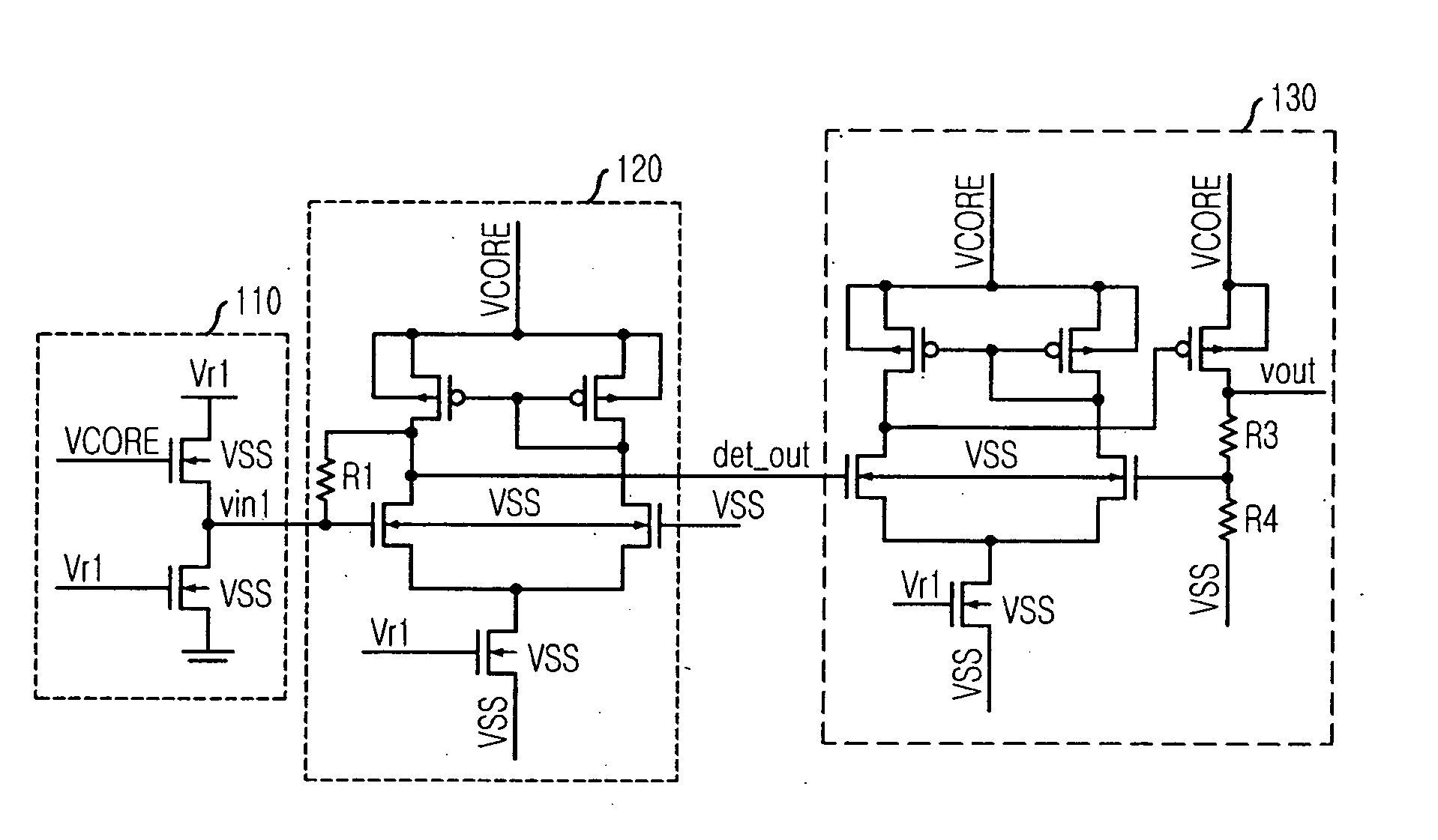
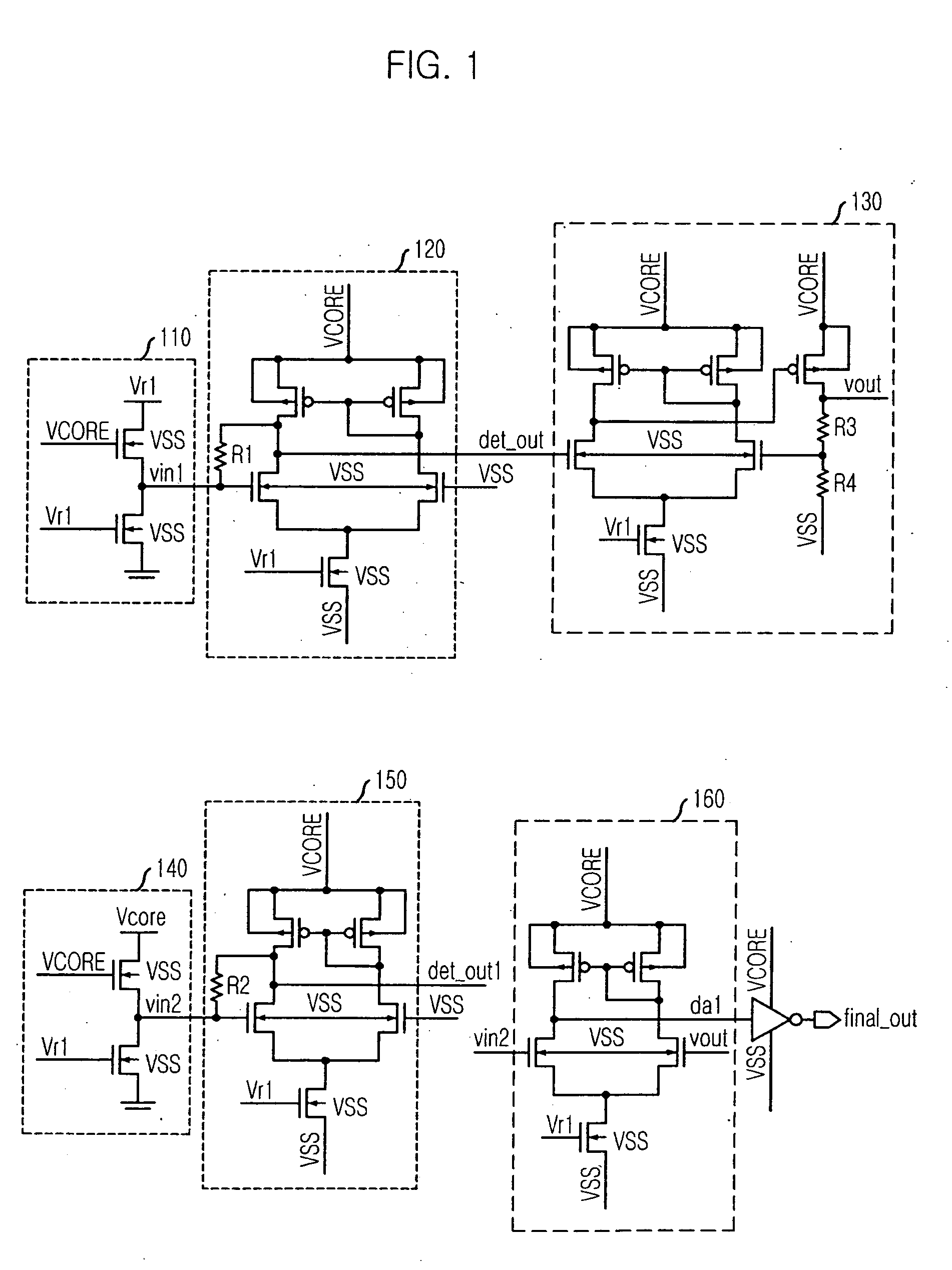
[0018] Referring to FIG. 1, there is shown a schematic diagram of a circuit for detecting skew of a transistor in accordance with the present invention.

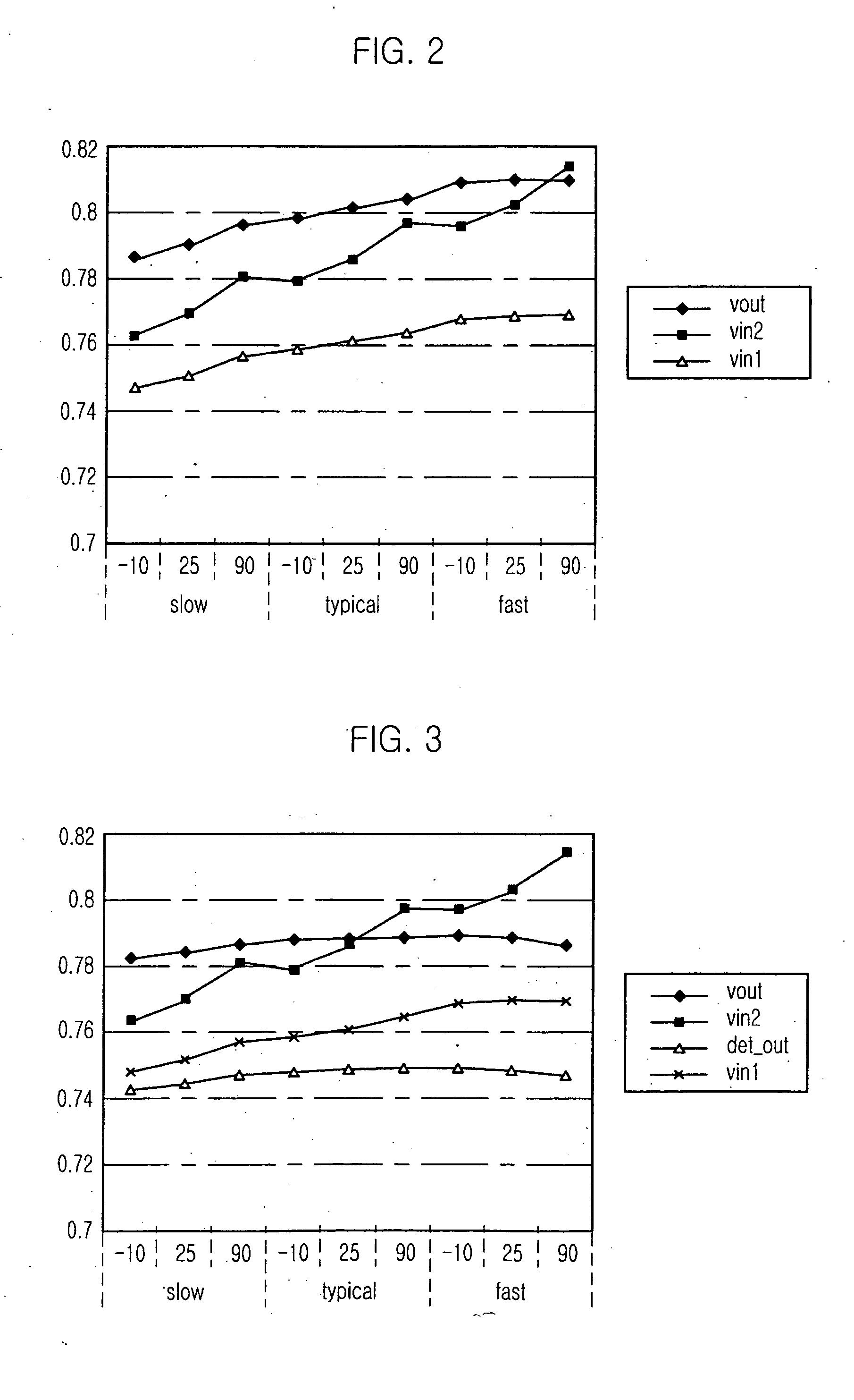
[0019] The skew detecting circuit includes a linear voltage generating unit 110 consisting of a plurality of switching devices connected to each other in series so as to output a linear voltage based on a first supply voltage Vr1, a first attenuation unit 120 for reducing variation width of the linear voltage according to temperature and skew by receiving the linear voltage through its inverting node and a ground voltage through its non-inverting node, and feeding back its output to the non-inverting node, a saturation voltage generating unit 140 consisting of a plurality of switching devices connected to each other in series to thereby output a saturation voltage based on a second supply voltag...


PUM

PropertyMeasurementUnit
linear voltageaaaaaaaaaa
widthaaaaaaaaaa
saturation voltageaaaaaaaaaa

Abstract

A circuit and method for easily detecting skew of a transistor within a semiconductor device are provided. The circuit for detecting the skew of the transistor includes a linear voltage generating unit for outputting a linear voltage by using a first supply voltage, a first attenuation unit for reducing variation width of the linear voltage according to the performance of the transistor, a saturation voltage generating unit for outputting a saturation voltage by using a second supply voltage, and a comparison unit for comparing an output of the first attenuation unit and the saturation voltage.

Description

FIELD OF THE INVENTION [0001] The present invention relates to a circuit for detecting skew of a transistor used in semiconductor memory devices. BACKGROUND OF THE INVENTION [0002] In general, as a semiconductor device is scaled down, property variation of a MOS transistor is getting larger according to skew and temperature since it is difficult to control device parameters and manufacturing processes which determine the performance of the MOS transistor. For instance, the manufacturing processes and device parameters include width and length of a transistor gate, thickness of a gate oxide, and a seat resistor and so on. As the size of the transistor is smaller, target values of those parameters become lower and, thus, tolerance to a target value of each process increases and the property variation of the transistor also becomes larger. Therefore, it is preferable that circuits within the semiconductor device are designed to operate without being effected by the variation of the tra...

Claims


Application Information

Patent Timeline
Patent Type & Authority Applications(United States)
IPC IPC(8): G11C7/00G11C16/04G11C29/50
CPCG11C29/12005G11C2029/5002G11C29/50B01D35/005B01D35/301B01D2201/304
Inventor HUR, HWANGCHOI, JUN-GI
Owner SK HYNIX INC
Why Eureka
Try Eureka