

Optical device
- Summary
- Abstract
- Description
- Claims
- Application Information
AI Technical Summary
Benefits of technology
Problems solved by technology
Method used
Image

Examples
first embodiment
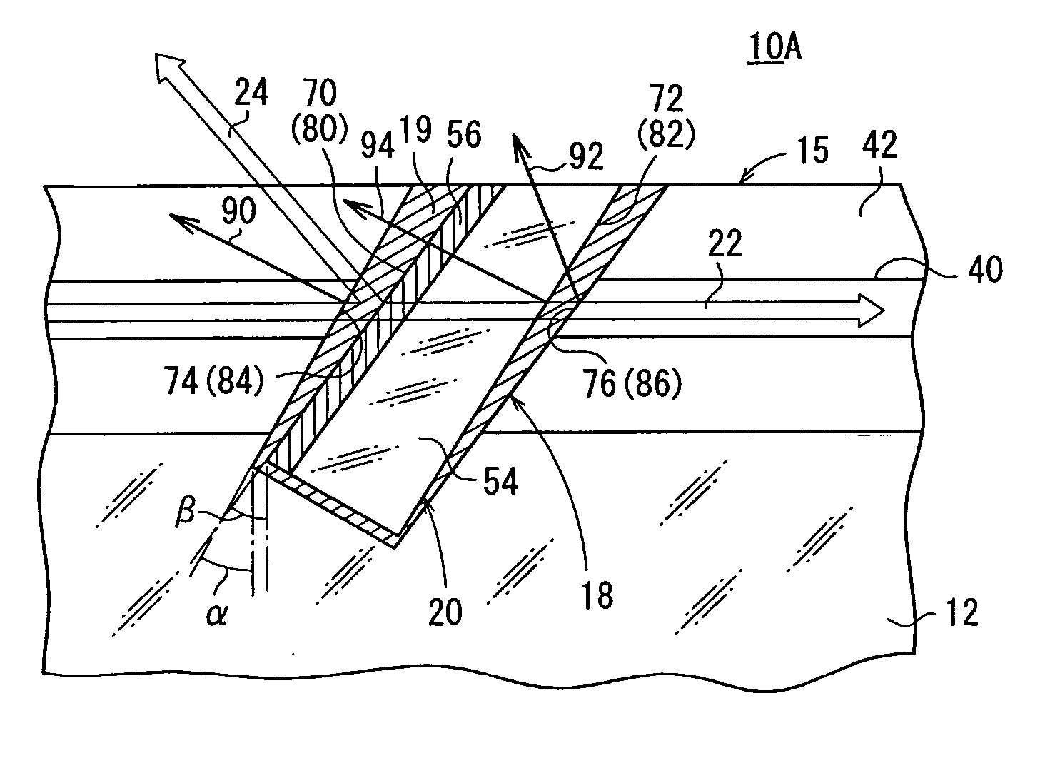
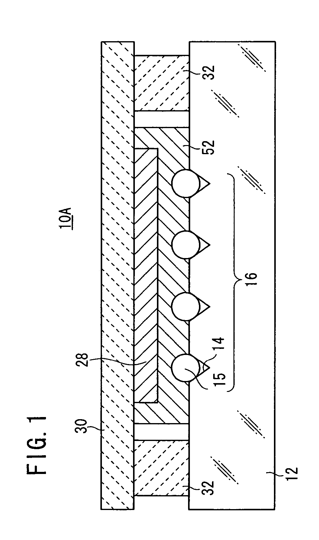
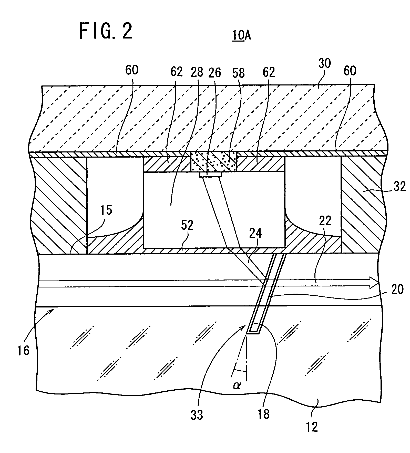
[0052] As shown in FIGS. 1 and 2, an optical device 10A has a glass substrate 12, an optical fiber array 16 comprising a plurality of optical fibers 15 fixed in a plurality of V-shaped grooves 14 defined in the glass substrate 12, a slit 18 (see FIG. 2) extending from respective upper surfaces of the optical fibers 15 into the glass substrate 12, a dividing member (filter member) 20 (see FIG. 2) inserted in the slit 18, a PD (PhotoDiode) array 28 having a plurality of active layers 26 for detecting light (reflected light) 24 reflected by at least the filter member 20, of signal light 22 passing through the optical fibers 15, a submount 30 fixing the PD array 28 so as to face the optical fiber array 16, and a spacer 32 for stably fixing at least the PD array 28. Two end faces of the slit 18 and face and reverse sides of the filter member 20 function as a divider 33 (see FIG. 2) for dividing part of signal light 22 that passes through the optical fibers 15. As shown in FIG. 3, each o...
second embodiment
[0089] An optical device 10B will be described below with reference to FIG. 13.
[0090] In the optical device 10B according to the second embodiment, as shown in FIG. 13, a line segment which is formed when the first surface 70 of the filter member 20 and a horizontal plane including the optical axis of the signal light 22 cross each other is defined as a fifth line segment 100, a line segment which is formed when the second surface 72 of the filter member 20 and the horizontal plane cross each other as a sixth line segment 102, a line segment which is formed when the first inner wall surface 74 of the slit 18 and the horizontal plane cross each other as a seventh line segment 104, and a line segment which is formed when the second inner wall surface 76 of the slit 18 and the horizontal plane cross each other as an eighth line segment 106. The seventh line segment 104 and the eighth line segment 106 lie parallel to each other, and the fifth line segment 100 and the seventh line segme...
third embodiment
[0093] An optical device 10C will be described below with reference to FIG. 14.
[0094] As shown in FIG. 14, the optical device 10C according to the third embodiment is of substantially the same structure as the optical device 10A according to the first embodiment. In particular, one common slit 18 is formed in and across an optical fiber array 16 comprising seven optical fibers 15, for example, and one filter member 20 is inserted in the slit 18, with the gap between the slit 18 and the filter member 20 within the slit 18 being filled with a resin 19.
[0095] The surface (first surface) 70 of the filter member 20 which confronts at least the first inner wall surface 74 of the slit 18 is curved concavely toward the first inner wall surface 74. The first surface 70 is curved to such an extent that difference between the central portion of the filter member 20 and the opposite ends thereof ranges from 5 μm to 100 μm. If the difference is smaller than 5 μm, then it is difficult to provid...
PUM
 Abstract
Description
Claims
Application Information