Backgated finfet having diferent oxide thicknesses

a backgated finfet and oxide thickness technology, applied in the direction of semiconductor devices, electrical apparatus, transistors, etc., can solve the problems of unsatisfactory leakage current between the source and drain, increased production costs, and increased production costs,

Inactive Publication Date: 2005-11-03
GLOBALFOUNDRIES INC
View PDF9 Cites 40 Cited by
  • Summary
  • Abstract
  • Description
  • Claims
  • Application Information

AI Technical Summary

Problems solved by technology

Single control of the channel often leads to undesired leakage current between the source and drain when the transistor is intended to be non-conductive.
This becomes especially problematic as the critical dimensions of integrated circuits continue to decrease.
Unfortunately, however, such planar double gate devices are difficult to manufacture.
However, increased impurity scattering by additional dopants may cause a significant degradation in mobility and drive current.
For example, the oxide may be damaged during etching of a dummy gate or during reactive ion etching (RIE) of the opposite side of a fin, which are integral steps of the SIT process.

Method used


Image

  • Backgated finfet having diferent oxide thicknesses
  • Backgated finfet having diferent oxide thicknesses
  • Backgated finfet having diferent oxide thicknesses

Examples


Embodiment Construction

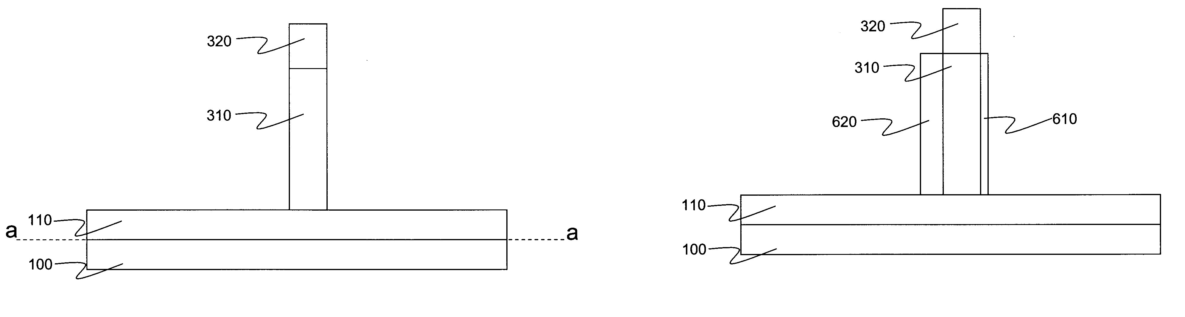
[0025] An exemplary process according to the invention involves steps of introducing impurities into at least one side of a fin of a FinFET to enable formation of dielectric layers with different thicknesses. The impurity, which may be introduced by implantation, either enhances or retards dielectric formation having a thicker dielectric layer in the back-gate (i.e., the biased non-switching gate) than in the front-gate thereby reducing front-gate to back-gate capacitance as well as source and drain to back-gate capacitance.

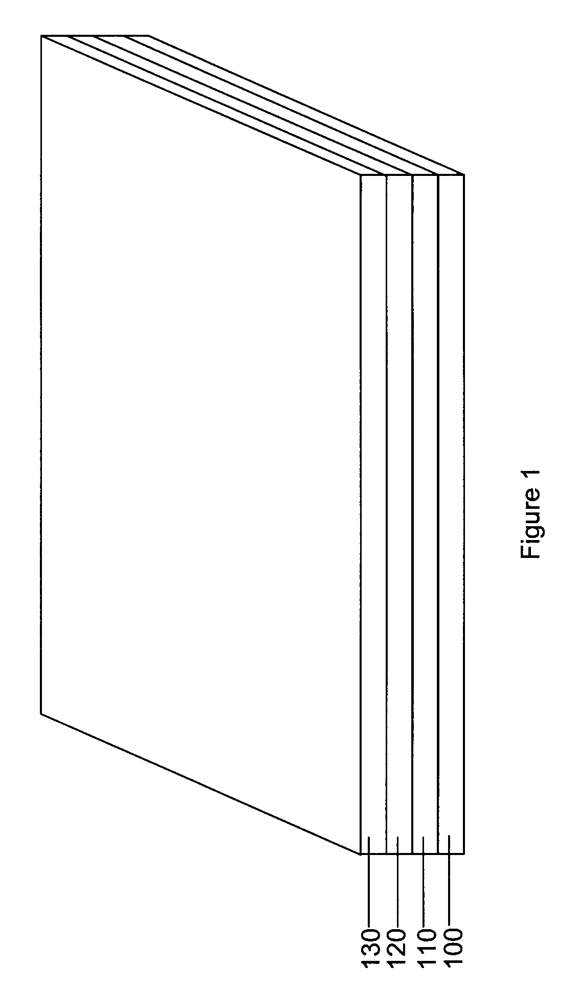
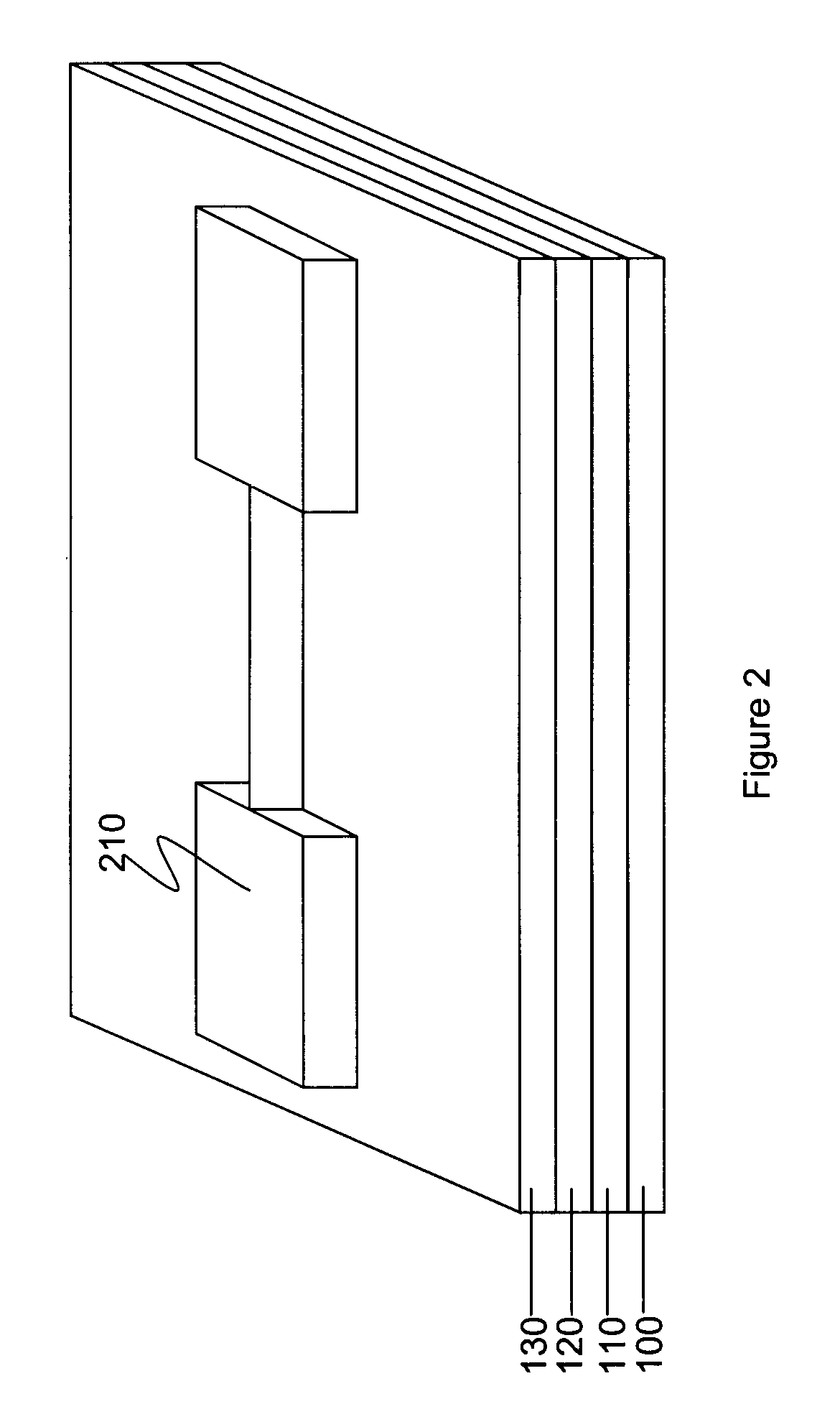
[0026] Referring now to FIG. 1, an exemplary substrate such as a silicon-on-insulator (SOI) structure is provided, including a silicon substrate layer 100, a buried oxide layer 110, and a silicon layer 120 on the buried oxide. The silicon layer 120 may, for example, have a thickness of approximately 50 nm, which determines the height of the fin (i.e., body of the transistor) to be formed, as described more fully below.

[0027] A hard mask 130 is formed in a conve...


PUM


Abstract

A method of producing a backgated FinFET having different dielectric layer thickness on the front and back gate sides includes steps of introducing impurities into at least one side of a fin of a FinFET to enable formation of dielectric layers with different thicknesses. The impurity, which may be introduced by implantation, either enhances or retards dielectric formation.

Description

BACKGROUND OF INVENTION [0001] The invention generally relates to a semiconductor device and method of manufacture and, more particularly, to a semiconductor device that includes FinFETs with different oxide thicknesses on front and back gates and a method of manufacture of such a device. [0002] Conventional metal oxide semiconductor field effect transistors (MOSFETs) have a single control gate on a planar substrate. Single control of the channel often leads to undesired leakage current between the source and drain when the transistor is intended to be non-conductive. This becomes especially problematic as the critical dimensions of integrated circuits continue to decrease. [0003] An improved planar structure employs two gates, one on each side of the channel. As this arrangement increases the electrostatic coupling between the gates and the channel, the drive current of the transistor is increased and the leakage current is decreased. Unfortunately, however, such planar double gate...

Claims


Application Information

Patent Timeline
Patent Type & Authority Applications(United States)
IPC IPC(8): H01L21/00H01L21/335H01L21/336H01L21/265H01L21/84H01L29/423H01L29/786
CPCH01L29/42368H01L29/785H01L29/66795H01L29/42384H01L29/7856
Inventor BRYANT, ANDRESDOKUMACI, OMER H.HANAFI, HUSSEIN I.NOWAK, EDWARD J.
Owner GLOBALFOUNDRIES INC
Why Eureka
Try Eureka