Copper damascene integration scheme for improved barrier layers

a technology of integrated circuits and copper damascenes, applied in semiconductor/solid-state device manufacturing, basic electric elements, electric apparatus, etc., can solve the problems of degrading device performance and reliability, increasing the possibility of copper migration under moderate temperatures and electrical fields to unacceptable values,

Inactive Publication Date: 2005-11-03
TAIWAN SEMICON MFG CO LTD
View PDF8 Cites 38 Cited by
  • Summary
  • Abstract
  • Description
  • Claims
  • Application Information

AI Technical Summary

Problems solved by technology

While several processing difficulties related to forming copper semiconductor features have been overcome, several problems remain, including the problem of barrier layer coverage and integrity to prevent copper migration as well as reducing signal delay caused by capacitive contributions of etch stop and barrier layers in a multi-layered integrated circuit.
One increasing problem with prior art methods of forming copper dual damascenes including barrier layers is achieving adequate coverage of the barrier layers over both the via and trench line portions of the dual damascene structure.
As a result, the probability for copper migration under moderate temperatures and electrical fields increases to unacceptable values, degrading device performance and reliability.

Method used


Image

  • Copper damascene integration scheme for improved barrier layers
  • Copper damascene integration scheme for improved barrier layers
  • Copper damascene integration scheme for improved barrier layers

Examples


Embodiment Construction

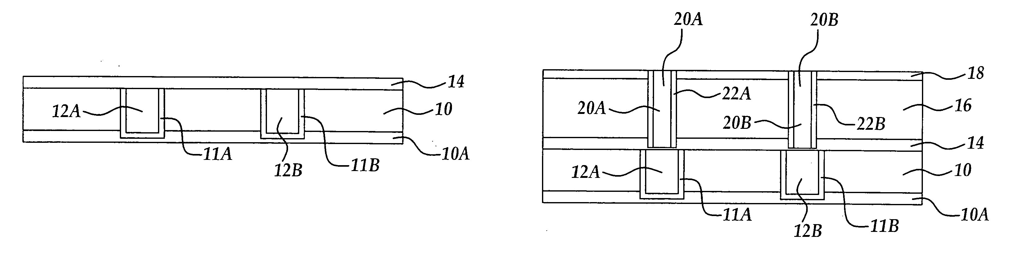
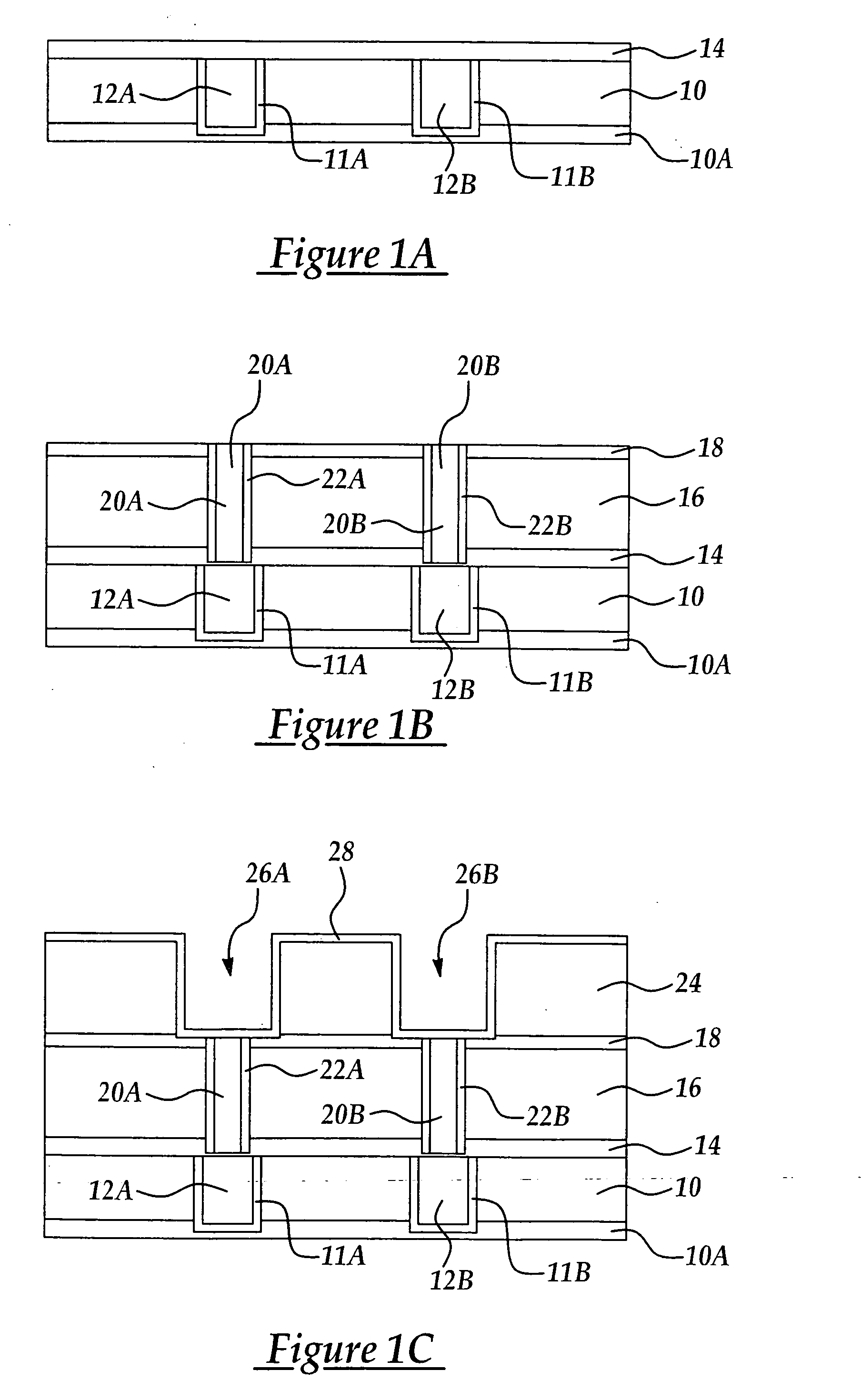
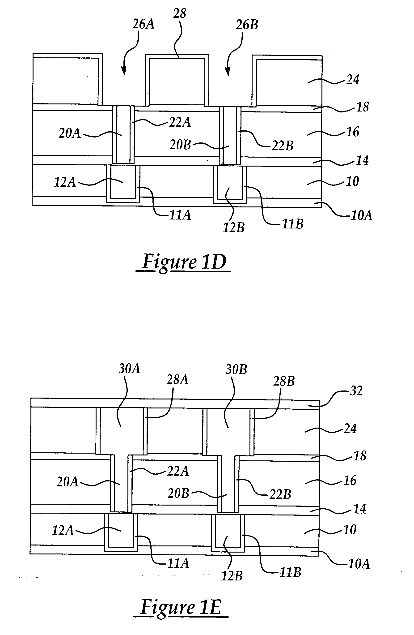
[0012] Although the method of the present invention is explained with reference to formation of an exemplary copper interconnect structure (feature) such as a dual damascene, it will be appreciated that the process may be equally as well used in forming single damascene structures overlying conductive areas well as thicker and wider structures such as bonding pads and wide trenches overlying conductive areas. Further, it will be appreciated that the metal used to fill the metal interconnect may additionally include tungsten and aluminum as well as copper and alloys thereof.

[0013] The method of the present invention is particularly advantageously used in the formation of copper dual damascene features including vias and trench lines for multi-layer semiconductor devices having characteristic dimensions of less than about 0.13 microns. In addition, the method is particularly advantageously used with organo-silicate glass (OSG) based low-K dielectric insulating layers and having a die...


PUM

PropertyMeasurementUnit
thicknessaaaaaaaaaa
dielectric constantaaaaaaaaaa
aspect ratiosaaaaaaaaaa

Abstract

A metal filled dual damascene structure with a reduced capacitance contribution and method for forming the same, the method including forming a first metal filled damascene lined with a first metal barrier layer thickness in a first dielectric insulating layer; and, forming a second metal filled damascene lined with a second metal barrier layer thickness overlying the first metal filled damascene in a second dielectric insulating layer.

Description

FIELD OF THE INVENTION [0001] This invention generally relates to methods for forming semiconductor device integrated circuits including copper damascene interconnects and more particularly to a method for forming copper dual damascenes to reduce signal delay and achieve improved barrier layer performance. BACKGROUND OF THE INVENTION [0002] Copper metallization is increasingly being used for advanced semiconductor device integrated circuit fabrication including semiconductor features having sub-quarter micron linewidths and high aspect ratios to larger features such as bonding pads. Copper and its alloys have lower resistivity and better electromigration resistance compared to other metals such as, for example, aluminum. These characteristics are critical for achieving device reliability together with higher current densities and increased signal propagation speed. While several processing difficulties related to forming copper semiconductor features have been overcome, several prob...

Claims


Application Information

Patent Timeline
Patent Type & Authority Applications(United States)
IPC IPC(8): H01L21/4763H01L21/768
CPCH01L21/76802H01L21/76831H01L21/76829
Inventor WU, ZHEN-CHENGLU, YUNG-CHENG
Owner TAIWAN SEMICON MFG CO LTD
Why Eureka
Try Eureka