High density LED array

Active Publication Date: 2005-11-10
SILICON VALLEY BANK
View PDF4 Cites 32 Cited by
  • Summary
  • Abstract
  • Description
  • Claims
  • Application Information

AI Technical Summary

Benefits of technology

[0011] Each such micro-reflector element has a lower portion and an upper portion. The upper portion is characterized by a packing edge having a selected perimeter shape. The perimeter shape, if responsive to the volumetric form, will be a circle, because this shape is the outline of any cross-section taken at the upper portion of an element having a volumetric form associated with a surface of revolution. Because circles do not pack as densely as may be desired and because, when packed, circles leave gaps there betwe

Problems solved by technology

Where the application requires delivery of a relatively high radiant power density at or across the work surface, a LED array may have some difficulty in that delivery.
However, even if close proximity delivers appropriate power density, this approach generally is undesirable because, e.g., close proximity tends to necessitate undesirable changes to tooling and/or shielding.
While this approach will tend to increase radiant power density, collecting and collimated a substantial preponderan

Method used


Image

  • High density LED array
  • High density LED array
  • High density LED array

Examples


Embodiment Construction

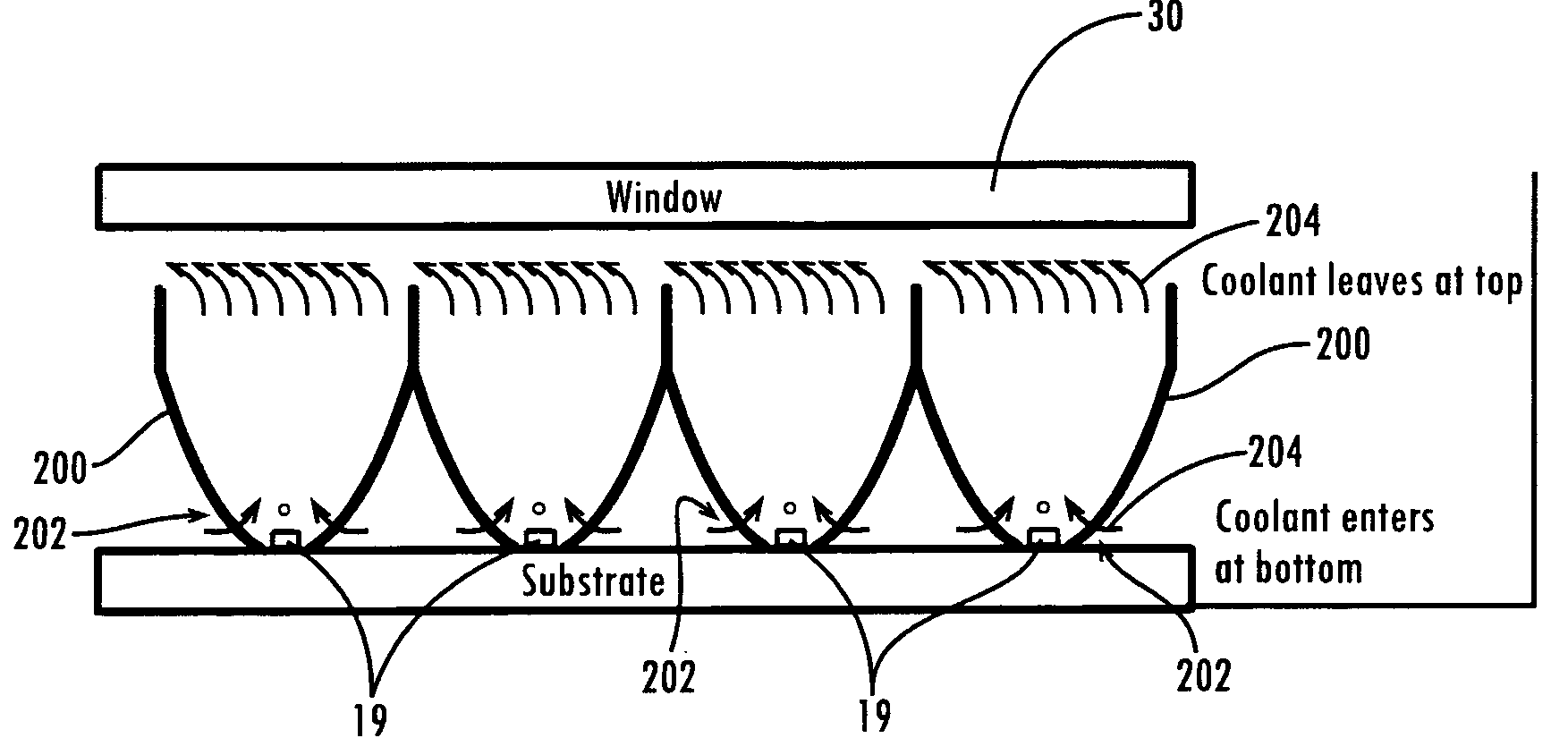
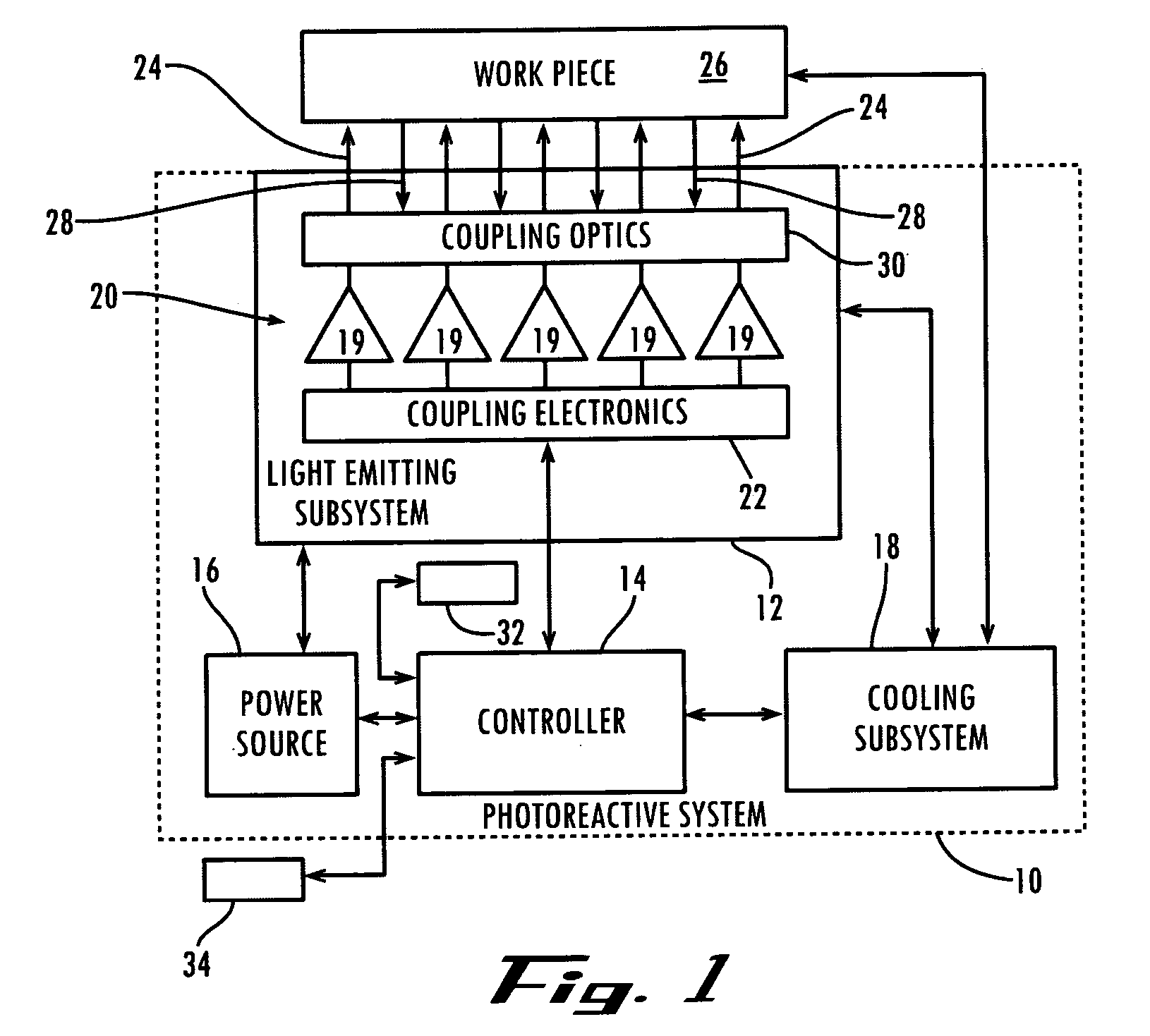
[0026]FIG. 1 is a block diagram of a photoreactive system 10 in accordance with the invention. In this example embodiment, the photoreactive system 10 comprises a light emitting subsystem 12, a controller 14, a power source 16 and a cooling subsystem 18.

[0027] The light emitting subsystem 12 preferably comprises a plurality of semiconductor devices 19. The semiconductor devices provide a radiant output 24. The radiant output 24 is directed to a work piece 26. Returned radiation 28 may be directed back to the light emitting system 12 from the work piece 26 (e.g., via reflection of the radiant output 24).

[0028] The radiant output 24 preferably is directed to the work piece 26 via coupling optics 30. The coupling optics 30 include a micro-reflector array. In employing such micro-reflector array, each semiconductor device providing radiant output 24 is associated with a respective micro-reflector element on a selected basis. As an example, each micro-reflector element of the array may...


PUM


Abstract

A dense array of semiconductor devices having an array of micro-reflectors, the micro-reflectors having characteristics that enhance dense packing of the array in balance with collection and collimation of the array's radiant output.

Description

RELATED APPLICATIONS [0001] This application claims priority from U.S. Provisional Application Ser. No. 60 / 561,771, filed Apr. 12, 2004, entitled “COLLIMATION AND DIRECT LIQUID COOLING OF HIGH-DENSITY LED ARRAYS”, the contents of which are hereby incorporated by reference, as if recited herein in full, for all purposes.BACKGROUND OF THE INVENTION [0002] This invention relates to high-density light emitting semiconductor device arrays and, more particularly, to a light emitting diode (LED) array having optical elements directed toward optimizing high-density packing of the LEDs in balance with collection and collimation of the LEDs' radiant output. [0003] Light-emitting semiconductor devices may be arranged in various configurations, such as arrays, for lighting applications. Examples of these applications include: lithographic processes used, e.g., in fabricating semiconductor devices, and curing processes used, e.g., for ink printing and fabrication of DVDs. These applications gene...

Claims


Application Information

Patent Timeline
IPC IPC(8): F21K99/00H01L25/075H01L33/60H01L33/64
CPCF21K9/00H01L25/0753H01L33/648H01L33/644H01L33/60H01L2924/0002H01L2924/00
Inventor OWENANDERSON, DUWAYNE R.
Owner SILICON VALLEY BANK
Why Eureka
Try Eureka