Display device

a display device and electroluminescence technology, applied in the direction of luminescence screens, discharge tubes, identification means, etc., can solve the problem of insufficient advantages of having top emission type configuration, and achieve the effect of maximizing the luminous area

Inactive Publication Date: 2005-11-17
JOLED INC
View PDF9 Cites 47 Cited by
  • Summary
  • Abstract
  • Description
  • Claims
  • Application Information

AI Technical Summary

Benefits of technology

[0020] According to the present invention, it is provided with a display device able to display an image in bright and high-definition by maximizing the area of the luminous region in the pixel.

Problems solved by technology

Consequently, only an advantage of having the top emission type configuration is not sufficient.

Method used


Image

  • Display device
  • Display device
  • Display device

Examples


first embodiment

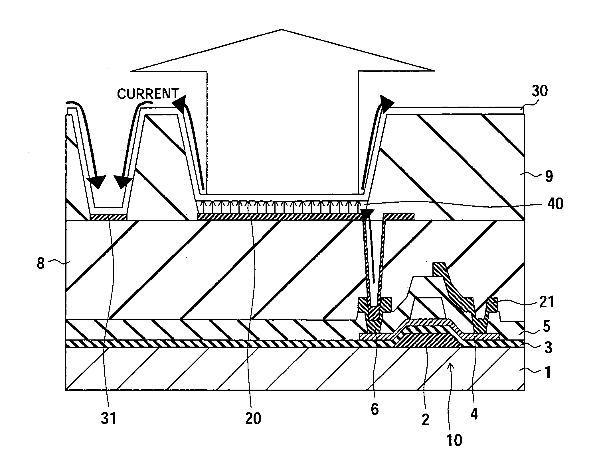
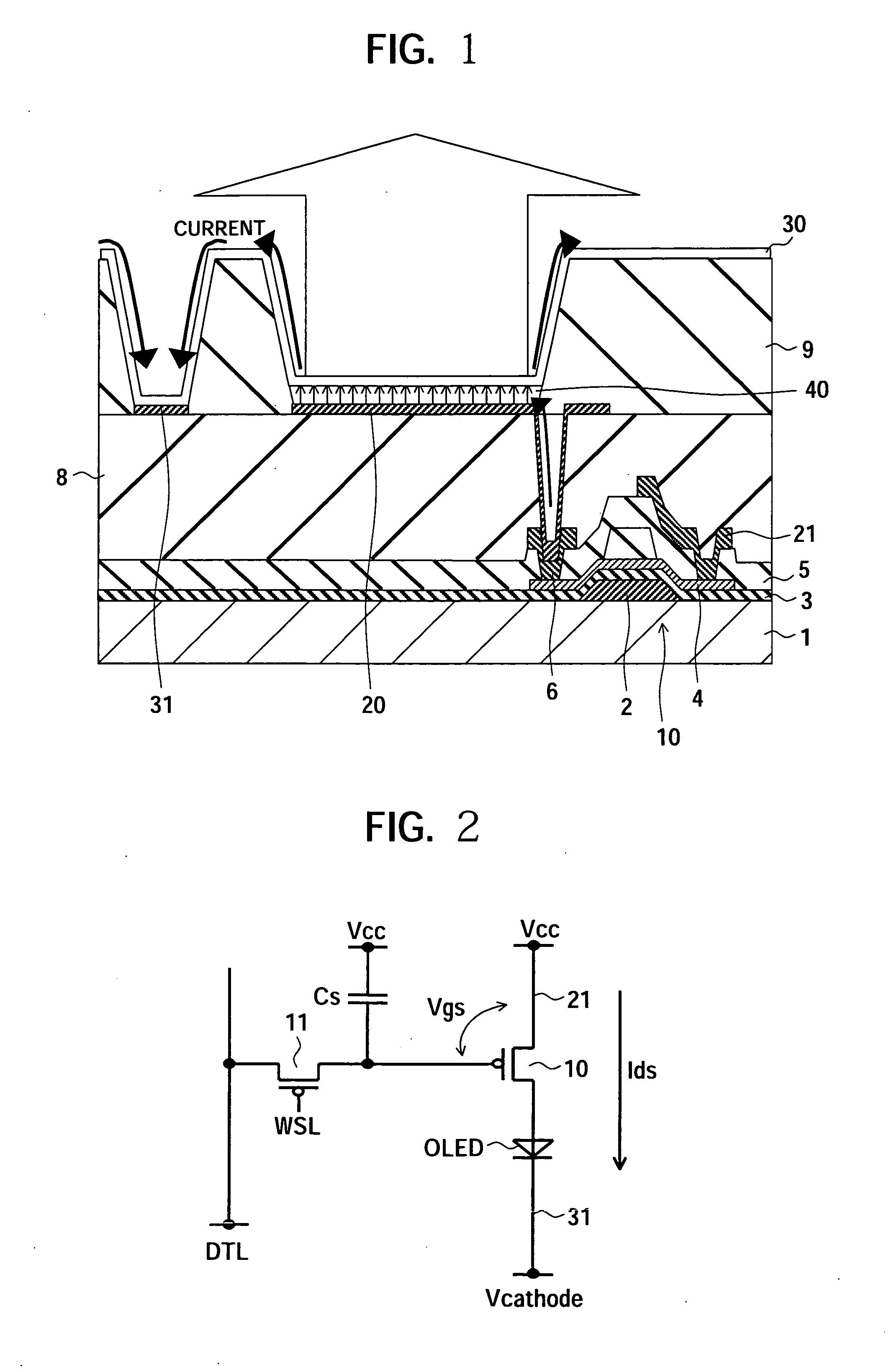
[0033]FIG. 1 is a general cross-sectional view of an organic electroluminescence display device according to the present embodiment.

[0034] The organic electroluminescence display device shown in FIG. 1 has an active matrix type configuration which drives a pixel by a thin film transistor 10 (hereinafter, referred to a “TFT”) formed on an insulation substrate 1.

[0035] The insulation substrate 1 is formed on its surface with a gate electrode 2 and the gate electrode 2 is covered with a gate insulation film 3 on the insulation substrate 1. The gate electrode 2 is formed with a semiconductor layer 4 of for example polysilicon via the gate insulation film 3. The semiconductor layer 4 is formed on its surface with an insulation film 5 and the insulation film 5 is formed on its surface with a drain electrode 6 which reaches the semiconductor layer 4 and an anode interconnection 21 to be a source electrode which reaches the semiconductor layer 4. A TFT 10 of, for example, a p-channel tran...


PUM


Abstract

A display device able to maximize an area of a luminous region in a pixel and realize an image display in bright and high-definition, wherein luminous elements having a first electrode defining a luminous region; a transparent second electrode facing and arranged to the first electrode; a luminous layer arranged between the first electrode and the second electrode are arranged in a first and second direction in matrix, a plurality of first electrode interconnections extending in the first direction and connected to a plurality of the first electrodes arranged in the first direction is arranged in the display region, and a plurality of second electrode interconnections arranged in parallel to the first electrode to extend in the second direction and commonly connected to a plurality of the second electrodes arranged in the second direction is also arranged.

Description

CROSS REFERENCES TO RELATED APPLICATIONS [0001] The present invention contains subject matter related to Japanese Patent Application JP 2004-145873 filed in the Japanese Patent Office on May 17, 2004, the entire contents of which being incorporated herein by reference. BACKGROUND OF THE INVENTION [0002] 1. Field of the Invention [0003] The present invention relates to an organic electroluminescence display device for example. [0004] 2. Description of the Related Art [0005] An active type organic electroluminescence display device has a configuration referred to a bottom emission type in related art. [0006] The configuration is characterized in that light of a luminous layer is emitted from a transparent substrate side formed with a thin film transistor performing a pixel drive to obtain an image. The luminous layer is sandwiched by a transparent electrode such as ITO formed at the transparent substrate side and a counter metal electrode in the respective pixels, and usually the coun...

Claims


Application Information

Patent Timeline
Patent Type & Authority Applications(United States)
IPC IPC(8): G09F9/30H01L51/50H01L27/32H05B33/14H05B33/26
CPCH01L27/3211H01L2251/5315H01L27/3297H01L27/3276H10K59/35H10K59/1315H10K59/131H10K2102/3026
Inventor FUJIMURA, HIROSHIINO, MASUMITSU
Owner JOLED INC
Why Eureka
Try Eureka