
CMOS-compatible light emitting aperiodic photonic structures

a photonic structure and amos technology, applied in the direction of active medium materials, semiconductor lasers, instruments, etc., can solve the problems of inability to achieve high-quality aperiodic structures, inability to achieve strong light-matter interaction and light emission, and standard materials approaches used to fabricate aperiodic photonic structures are not suited to achieve strong light emission homogeneously from all the layers of the structur

Inactive Publication Date: 2005-11-17
MASSACHUSETTS INST OF TECH
View PDF8 Cites 32 Cited by
  • Summary
  • Abstract
  • Description
  • Claims
  • Application Information

AI Technical Summary

Benefits of technology

The present invention is related to a method for fabricating a periodic structure using thin film layers of SiO2 and SiNx. The method involves depositing layers of SiO2 and SiNx onto a substrate and annealing them to form the structure. The resulting structure has fractal cavities and can be used in light emitting devices and photonic quasicrystal planar devices. The technical effects of this invention include improved optical properties and more efficient light emitting devices.

Problems solved by technology

More challenging is the fabrication of high quality aperiodic structures.
However, despite the big potential of aperiodic structures for enhancing light-matter interactions, no such aperiodic structures have been demonstrated combining both strong light-matter interaction and light emission.
In fact, the standard materials approaches used to fabricate aperiodic photonic structures are not suited to obtain strong light emission homogeneously from all the layers constituting the structures.
In other words, conventional materials used to fabricate aperiodic structures do not provide efficient light emission originating homogeneously from within the photonic structure itself.

Method used


Image

  • CMOS-compatible light emitting aperiodic photonic structures
  • CMOS-compatible light emitting aperiodic photonic structures
  • CMOS-compatible light emitting aperiodic photonic structures

Examples


Embodiment Construction

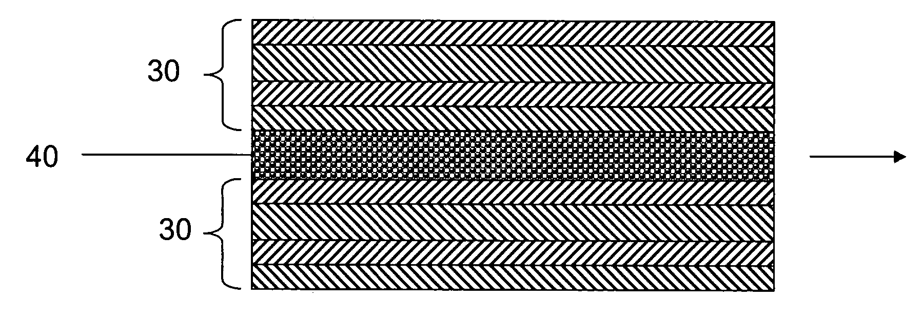
[0023] The present invention will be described in connection with preferred embodiments; however, it will be understood that there is no intent to limit the present invention to the embodiments described herein. On the contrary, the intent is to cover all alternatives, modifications, and equivalents as may be included within the spirit and scope of the present invention as defined by the appended claims.

[0024] For a general understanding of the present invention, reference is made to the drawings. In the drawings, like reference numbering has been used throughout to designate identical or equivalent elements. It is also noted that the various drawings illustrating the present invention may not have been drawn to scale and that certain regions may have been purposely drawn disproportionately so that the features and concepts of the present invention could be properly illustrated.

[0025] As noted above, the present invention is directed to light emitting optical devices characterized...


PUM


Abstract

A fabrication method and materials produce high quality aperiodic photonic structures. Light emission can be activated by thermal annealing post growth treatments when thin film layers of SiO2 and SiNx or Si-rich oxide are used. From these aperiodic structures, that can be obtained in different vertical and planar device geometries, the presence of aperiodic order in a photonic device provides strong group velocity reduction (slow photons), enhanced light-matter interaction, light emission enhancement, gain enhancement, and / or nonlinear optical properties enhancement.

Description

PRIORITY INFORMATION [0001] The present patent application claims priority under 35 U.S.C. §119 from U.S. Provisional Patent Application Ser. No. 60 / 565,164, filed on Apr. 23, 2004; from U.S. Provisional Patent Application Ser. No. 60 / 564,900, filed on Apr. 23, 2004; and from U.S. Provisional Patent Application Ser. No. 60 / 631,041, filed on Nov. 24, 2004. The entire contents of U.S. Provisional Patent Application Ser. No. 60 / 565,164, filed on Apr. 23, 2004; U.S. Provisional Patent Application Ser. No. 60 / 564,900, filed on Apr. 23, 2004; and U.S. Provisional Patent Application Ser. No. 60 / 631,041, filed on Nov. 24, 2004, are hereby incorporated by reference.GOVERNMENT RIGHTS NOTICE [0002] The present invention was made with government support under Grant (Contract) Number, DMR 02-13282, awarded by the National Science Foundation. The US Government has certain rights to this invention.FIELD OF THE PRESENT INVENTION [0003] The present invention is directed to light emitting aperiodic p...

Claims


Application Information

Patent Timeline
Patent Type & Authority Applications(United States)
IPC IPC(8): G02B6/122H01L21/00H01L21/31H01L21/314H01L21/469H01L21/76H01L33/46H01S3/06H01S3/063H01S3/083H01S3/16H01S5/10H01S5/183
CPCB82Y10/00H01S5/183G02B6/1225H01L21/3144H01L33/46H01S3/0604H01S3/0627H01S3/0632H01S3/0637H01S3/083H01S3/0933H01S3/0941H01S3/16H01S3/1603H01S3/1628H01S3/169H01S5/105B82Y20/00H01S5/11H01L21/0217H01L21/0214H01L21/02164H01L21/02274H01L21/02337
Inventor NEGRO, LUCA DALYI, JAE HYUNGMICHEL, JURGENYI, YASHANGUYEN, VICTOR T.KIMERLING, LIONEL C.
Owner MASSACHUSETTS INST OF TECH
Learn More