Method of fabricating organic light emitting display

Inactive Publication Date: 2005-12-01
SAMSUNG DISPLAY CO LTD
9 Cites 22 Cited by

AI-Extracted Technical Summary

Problems solved by technology

Therefore, forming the top emission OLED and the bottom emission OLED on a single substrate complicates the fabrication process.
To solve at least the ab...

Method used

[0038] The reflecting layer is etched by photolithography process and forms a first reflecting layer pattern 280 in an emission region of the first region A. The first reflecting layer pattern 280 reflects light in the first region A to increase luminance and light efficiency. The first reflecting layer 280 is not formed in the second region B.
[0045] The second reflecting layer pattern 288 is formed to approximately 100 to 3000 Å thick. The second reflecting layer pattern 288 is preferably formed to 500 to 2500 Å thick. The second reflecting layer pattern 288 may be formed by a thermal deposition method, a sputtering method, or the like. The second reflecting layer pattern 288 is preferably formed by a sputtering method to ...

Benefits of technology

[0024] The present invention provides a method of fabricating an OLED that simplifies a fabrication process by simultaneously forming an opposite electrode using a same material in a top emission re...

Abstract

A method of fabricating an organic light emitting display is provided, in which, a first electrode is formed above a substrate having first and second regions, respectively, an emission layer is formed in the first and second regions, a second electrode is formed on the emission layer in the first and second regions, and a reflecting layer pattern is selectively formed on the second electrode in the second region.

Application Domain

Technology Topic

Image

  • Method of fabricating organic light emitting display
  • Method of fabricating organic light emitting display
  • Method of fabricating organic light emitting display

Examples

  • Experimental program(1)

Example

[0031] Reference will now be made in detail to the embodiments of the present invention, examples of which are illustrated in the accompanying drawings, wherein like reference numerals refer to the like elements throughout. The embodiments are described below in order to explain the present invention by referring to the figures.
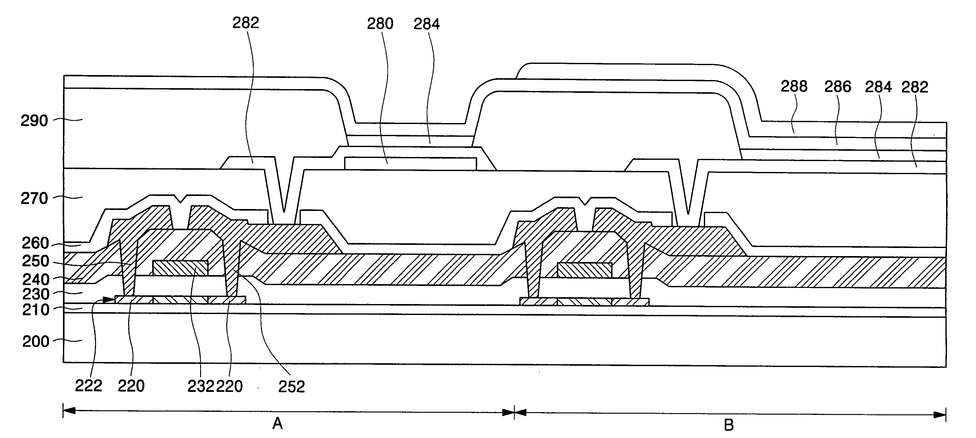
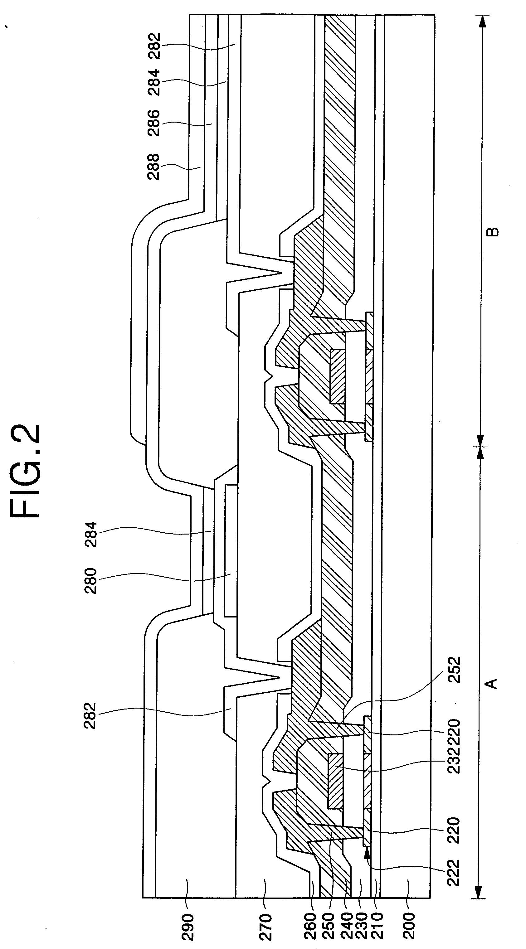
[0032]FIG. 2 is a cross-sectional view of an OLED according to an embodiment of the invention. It is understood that the invention is not limited to the embodiment shown in FIG. 2. Referring to FIG. 2, the OLED of FIG. 2 includes a first region A and a second region B. The processes discussed below are simultaneously performed in the first and second regions A and B unless otherwise described. However, it is understood that the processes formed in the first and second regions A and B do not need to be performed simultaneously.
[0033] A buffer layer 210 having a predetermined thickness is provided or formed on a substrate 200 having a thin film transistor (TFT) formed thereon. The TFT includes a polysilicon pattern 222, a gate electrode 232, and source and drain electrodes 250 and 252 formed thereon. The source and drain regions 220 into which impurities are doped are provided at opposite sides of the polysilicon pattern 222, and a gate insulating layer 230 is formed on the entire surface of the structure and covers the polysilicon pattern 222.
[0034] A passivation layer 260 having a predetermined thickness is subsequently formed on the entire surface of the structure. The passivation layer 260 is etched by a photolithography process and forms a first via contact hole (not shown) thereon that exposes one of the source and drain electrodes 250 and 252, for example, the drain electrode 252. The passivation layer 260 may be formed of a silicon oxide layer, a silicon nitride layer, or a stacked layer thereof.
[0035] A first insulating layer 270 is formed on the entire surface of the structure. The first insulating layer 270 may be made from polyimide, benzocyclobutene-series resin, spin on glass (SOG), or acrylate. The first insulating layer 270 is subsequently formed over the emission region, e.g., planarizes the emission region.
[0036] The first insulating layer 270 is subsequently etched by a photolithography process and forms a second via contact hole (not shown) is formed thereon that exposes the first via contact hole.
[0037] A reflecting layer (not shown) is subsequently formed on an entire upper surface of the structure. The reflecting layer is made of a material having a high reflectivity, such as aluminum (Al), an aluminum alloy, molybdenum (Mo), titanium (Ti), gold (Au), silver (Ag), palladium (Pd), and the like.
[0038] The reflecting layer is etched by photolithography process and forms a first reflecting layer pattern 280 in an emission region of the first region A. The first reflecting layer pattern 280 reflects light in the first region A to increase luminance and light efficiency. The first reflecting layer 280 is not formed in the second region B.
[0039] A thin layer for a pixel electrode (not shown) is subsequently formed on an entire upper surface of the structure. The pixel electrode thin layer is made of a transparent metal material, such as indium thin oxide (ITO).
[0040] The pixel electrode thin layer is etched by photolithography process to form a pixel electrode 282 in each of the first and second regions A and B. The pixel electrode 282 contacts one of the source and drain electrodes 250 and 252 that is exposed by the second via contact hole, for example, the drain electrode 152. As shown in FIG. 2, for example, the pixel electrode 282 in the first region A has a dual layer structure that includes the first reflecting layer pattern 280 and the pixel electrode 282. It is understood that an additional process may be performed so that the pixel electrode 282 in the first region A has a different thicknesses than the pixel electrode 282 in the second region B.
[0041] A second insulating layer (not shown) is subsequently formed on an entire upper surface of the structure. The second insulating layer may be made of, for example, polyimide, benzocyclobutene-series resin, phenol-series resin, or acrylate. The second insulating layer is etched by photolithography process and forms a second insulating layer pattern 290.
[0042] An emission layer 284 is subsequently formed in the emission region. The emission layer 284 may be formed using a low molecular deposition method, a laser induced thermal imaging method, or the like. The emission layer 284 includes an organic emission layer and at least one of an electron injection layer, an electron transport layer, a hole injection layer, a hole transport layer, and a hole blocking layer.
[0043] An opposite electrode 286 is subsequently formed on an entire upper surface of the structure. The opposite electrode 286 is formed having a thickness of approximately 10 to 100 Å in both of the first and second regions A and B. The opposite electrode 286 may be formed of a transparent metal layer, such as an Mg—Ag layer, a Ca—Ag layer, or a Ba—Ag layer.
[0044] A second reflecting layer pattern 288 is subsequently formed on or above the opposite electrode 286 in the second region B using a mask that exposes the second region B. The second reflecting layer pattern 288 may be formed of a metal layer having a high reflectivity, e.g., an aluminum (Al) layer, a silver (Ag) layer, a gold (Au) layer, a palladium (Pd) layer, and/or an alloy thereof.
[0045] The second reflecting layer pattern 288 is formed to approximately 100 to 3000 Å thick. The second reflecting layer pattern 288 is preferably formed to 500 to 2500 Å thick. The second reflecting layer pattern 288 may be formed by a thermal deposition method, a sputtering method, or the like. The second reflecting layer pattern 288 is preferably formed by a sputtering method to reduce a fabrication process time. The second reflecting layer pattern 288 may be formed using the sputtering method because the opposite electrode 286 is approximately 10 to 100 Å thick. Further, the opposite electrode in the second region B is a stacked structure of the opposite electrode 286 and the second reflecting layer pattern 288.
[0046] A transparent sealing substrate is subsequently applied or provided on the opposite electrode, thereby completing the fabrication of the OLED.
[0047] As described above, according to the present invention, an opposite electrode is formed using the same material in the top emission region and the bottom emission region by a single process, thereby simplifying a fabrication process, reducing a fabrication time, and increasing fabrication output without adversely affecting the electrical and/or optical characteristics of the display.
[0048] Although a few embodiments of the present invention have been shown and described, it would be appreciated by those skilled in the art that changes may be made in these embodiments without departing from the principles and spirit of the invention, the scope of which is defined in the claims and their equivalents.

PUM

no PUM

Description & Claims & Application Information

We can also present the details of the Description, Claims and Application information to help users get a comprehensive understanding of the technical details of the patent, such as background art, summary of invention, brief description of drawings, description of embodiments, and other original content. On the other hand, users can also determine the specific scope of protection of the technology through the list of claims; as well as understand the changes in the life cycle of the technology with the presentation of the patent timeline. Login to view more.

Similar technology patents

Heat sink fabrication method

InactiveUS20130319064A1Simplify fabrication processReduce tooling costSemiconductor/solid-state device detailsSolid-state devicesHeat sinkRadiation
Owner:DONG GUAN YUNG TENG ELECTRONICS PROD

Method for fabricating memory device

ActiveUS9070753B1Reduce process variation and fabricating costSimplify fabrication processSolid-state devicesSemiconductor/solid-state device manufacturingPhysicsMask layer
Owner:MACRONIX INT CO LTD

Variable optical attenuator

InactiveUS20050013580A1Compact sizeSimplify fabrication processCoupling light guidesPiezoelectric/electrostrictive devicesEngineeringElastomer
Owner:LG ELECTRONICS INC

Projection system and light-homogenizing device adjustment element

ActiveUS20140185022A1Decrease number of componentSimplify fabrication processProjectorsColor television detailsProjection systemActuator
Owner:CORETRONIC

Classification and recommendation of technical efficacy words

Why Eureka
Try Eureka