Plasma display module and method of manufacturing the same

a technology of display module and display module, which is applied in the manufacture of electric discharge tube/lamp, identification means, instruments, etc., can solve the problems of increasing manufacturing costs and achieve the effect of improving the light emission efficiency

Inactive Publication Date: 2005-12-01
SAMSUNG SDI CO LTD
View PDF13 Cites 18 Cited by
  • Summary
  • Abstract
  • Description
  • Claims
  • Application Information

AI Technical Summary

Benefits of technology

[0022] It is therefore and object of the present invention to provide...

Problems solved by technology

Various equipments can lead to product failures while transferring from one process to another or while aligning the ...

Method used


Image

  • Plasma display module and method of manufacturing the same
  • Plasma display module and method of manufacturing the same
  • Plasma display module and method of manufacturing the same

Examples


first embodiment

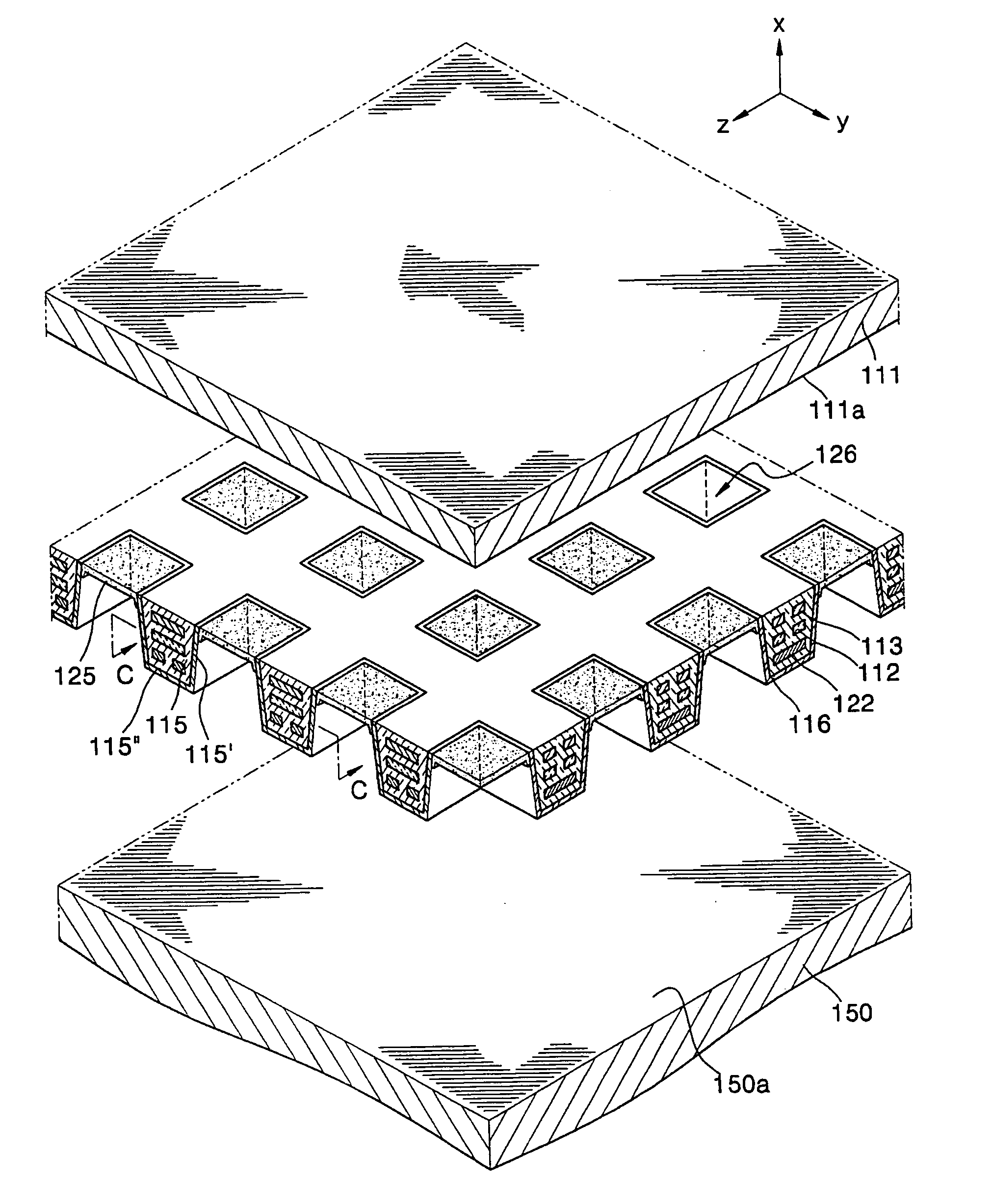
[0066] A plasma display module according to the present invention will now be described with reference to FIGS. 3 through 8.

[0067] The plasma display module includes a substrate 111, a chassis base 150, a plurality of barrier ribs 115, an MgO film 116, a plurality of front discharge electrodes 113, a plurality of rear discharge electrodes 112, a plurality of address electrodes 122, a fluorescent layer 125, a discharge gas, and circuit substrates 61, 62, 63, 64, 65, and 66.

[0068] The chassis base 150 is formed of an insulator, such as a plastic, and disposed on a rear side of the substrate 111. The insulator can be formed of a material having a resistance to transformation by heat generated by a discharge occurring in a discharge cell 126, which will be described later, and high thermal conductivity. Also, a front surface of the chassis base 150 is preferably flat since it defines discharge cells 126 by coupling with the substrate 111.

[0069] The chassis base 150 supports the circui...

second embodiment

[0131] A plasma display module will now be described with reference to FIGS. 23 through 27.

[0132] The plasma display module includes a substrate 411, a chassis base 450, a plurality of barrier ribs 415, an MgO film 416, a plurality of front discharge electrodes 413, a plurality of rear discharge electrodes 412, a plurality of address electrodes 422, a fluorescent layer 425, a discharge gas, and a plurality of circuit substrates 61, 62, 63, 64, 65, and 66.

[0133] The chassis base 450 is formed of an insulator, such as plastic, and is disposed on a rear (−X direction) of the substrate 411. The insulator can be formed of a material having a resistance to heat generated by a discharge in a discharge cell 426 and high thermal conductivity. Also, a front surface 450a of the chassis base 450 is flat since the chassis base 450 defines discharge cells 426 by coupling with the substrate 411.

[0134] The chassis base 450 supports the circuit substrates 61, 62, 63, 64, 65, and 66 disposed on a ...

second modified embodiment

[0174] A second modified version of the second embodiment with respect to mainly the difference from the second embodiment will now be described with reference to FIG. 29. The difference of the present second modified embodiment from the second embodiment is that address electrodes 622 are formed on an upper surface 450a of the chassis base 450.

[0175] The address electrodes 622 are extended to cross front discharge electrodes 613 and rear discharge electrodes 612 extended in a direction, and are covered by a dielectric layer 623. The barrier ribs 415 and the fluorescent layer 425 are formed on a front surface 623a of the dielectric layer 623.

[0176] The plasma display module according to the present second modified embodiment of the second embodiment is manufactured in the following method. The method includes: (a) preparing a substrate 411 formed of a transparent insulator and a chassis base 450 formed of an insulator; (b) forming address electrodes 622 on a front surface 450a of t...


PUM


Abstract

A plasma display module that can improve the emission efficiency of light, generate a discharge quickly, reduce an address voltage, and be manufactured at lower costs and failure rates, includes a substrate formed of a transparent insulator, a chassis base disposed on a rear side of the substrate, a plurality of barrier ribs formed of a dielectric disposed between the substrate and the chassis base and define discharge cells together with the substrate and the chassis base, a plurality of front discharge electrodes formed in the barrier ribs that surround the discharge cell, a plurality of rear discharge electrodes spaced apart from the front discharge electrodes and formed in the barrier ribs to surround the discharge cell, a fluorescent layer disposed in the discharge cell, a discharge gas filled in the discharge cell, and a plurality of circuit substrates that apply electrical signals to the electrodes by disposing on a rear side of the chassis base.

Description

CLAIM OF PRIORITY [0001] This application makes reference to, incorporates the same herein, and claims all benefits accruing under 35 U.S.C. §119 from an application for PLASMA DISPLAY MODULE AND METHOD FOR MANUFACTURING THE SAME earlier filed in the Korean Intellectual Property Office on 27 May 2004 and there duly assigned Ser. No. 10-2004-0037671. BACKGROUND OF THE INVENTION [0002] 1. Field of the Invention [0003] The present invention relates to a plasma display module. [0004] 2. Description of the Related Art [0005] A plasma display module is a display device on which a predetermined image is displayed using light emitted from fluorescent materials excited by ultraviolet rays generated by a gas discharge. It is expected to be a next generation display device since a thin and wide displaying surface can be produced. [0006]FIG. 1 is a perspective view of a conventional plasma display module. The plasma display module includes a PDP (plasma display panel) 1 that includes a front pa...

Claims


Application Information

Patent Timeline
IPC IPC(8): G09F9/313H01J9/24H01J17/49
CPCH01J9/241H01J11/46H01J11/16H01J11/22H01J11/36H01J11/40H01J17/16
Inventor WOO, SEOK-GYUNKANG, KYOUNG-DOOHONG, CHONG-GI
Owner SAMSUNG SDI CO LTD
Why Eureka
Try Eureka