Optical device having optical waveguide and method for manufacturing the same

a technology of optical waveguides and optical devices, which is applied in the direction of optical waveguide light guides, optical light guides, instruments, etc., can solve the problems of limited thickness of siosub>2 /sub>layers, and the loss of connection loss between the waveguide and the optical source becomes larger, so as to reduce the loss of connection light between the device and the light source, the column height can be increased and the effect of reducing the loss of ligh

Active Publication Date: 2005-12-01
DENSO CORP
View PDF6 Cites 9 Cited by
  • Summary
  • Abstract
  • Description
  • Claims
  • Application Information

AI Technical Summary

Benefits of technology

[0005] In view of the above-described problem, it is an object of the present invention to provide an optical device having an optical waveguide with low connection loss of light.
[0006] It is another object of the present invention to provide a method for manufacturing an optical device having an optical waveguide with low connection loss of light.
[0008] In the above device, an average refraction index in the column becomes larger as it goes to a top of the column so that the light is trapped effectively in the device. Further, the height of the column can be increased so that connection loss of light between the device and a light source is reduced.
[0012] The above method provides the device, in which an average refraction index in the column becomes larger as it goes to a top of the column so that the light is trapped effectively in the device. Further, the height of the column can be increased so that connection loss of light between the device and a light source is reduced.
[0014] The above method provides the device, in which an average refraction index in the column becomes smaller as it goes to a top or a bottom of the column so that the light is trapped effectively in the device. Further, the height of the column can be increased so that connection loss of light between the device and a light source is reduced.

Problems solved by technology

The deposition of a SiO2 layer as the core layer has a limitation so that the thickness of the SiO2 layer is limited.
Therefore, connection loss at a connection between the waveguide and an optical source becomes larger.

Method used


Image

  • Optical device having optical waveguide and method for manufacturing the same
  • Optical device having optical waveguide and method for manufacturing the same
  • Optical device having optical waveguide and method for manufacturing the same

Examples


first embodiment

[0033] The inventors have preliminarily studied about an optical device having an optical waveguide. FIG. 15 shows the waveguide as an example. The device includes a silicon substrate 100, a cladding layer 101 on the substrate 100, and a core layer 102 as an optical waveguide. The core layer 102 is disposed on the substrate 100 through the cladding layer 101. The core layer 102 is formed to have a predetermined pattern. In the device, a light wave is introduced from A-direction into the core layer 102, and then, the light wave is divided into two directions. Then, two light waves are outputted toward B- and C-directions.

[0034] Further, the device includes a passive element such as a prism and an optical filter and a positive element such as a semiconductor laser so that a planer light wave circuit (i.e., PCL) including an electric integrated circuit is formed.

[0035] Here, the optical device having the waveguide is similar to an optical fiber on a substrate. Therefore, two differen...

second embodiment

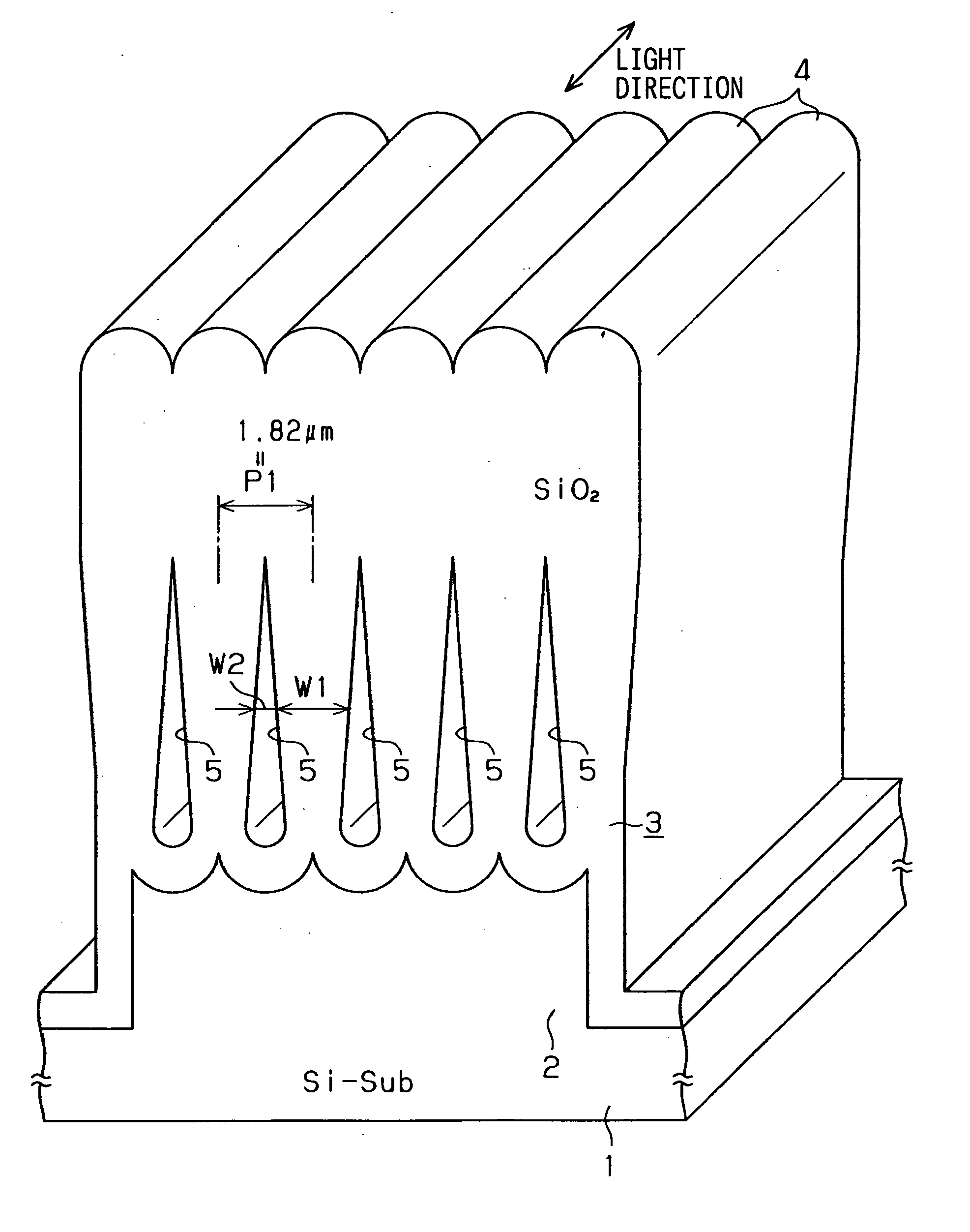
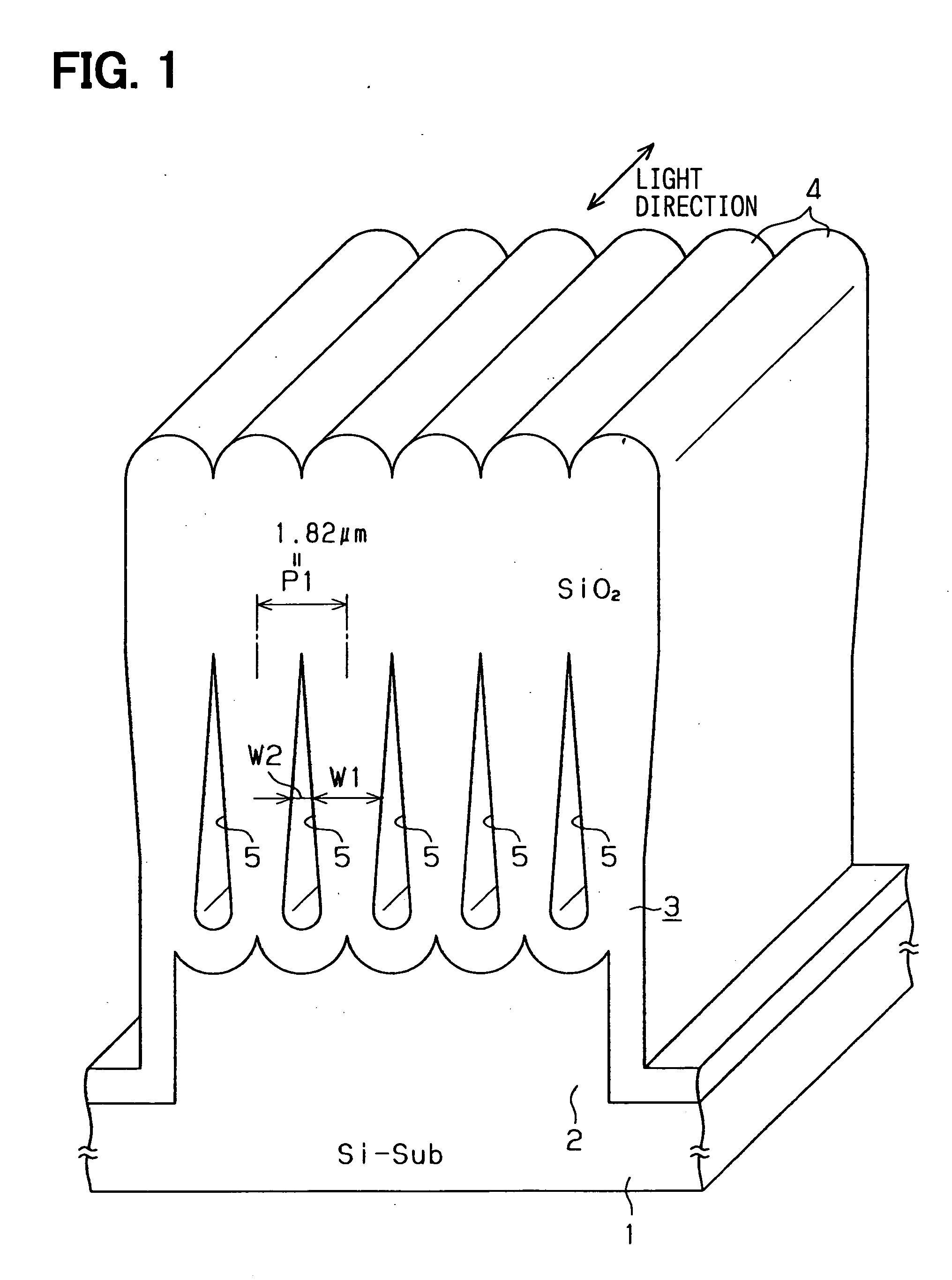
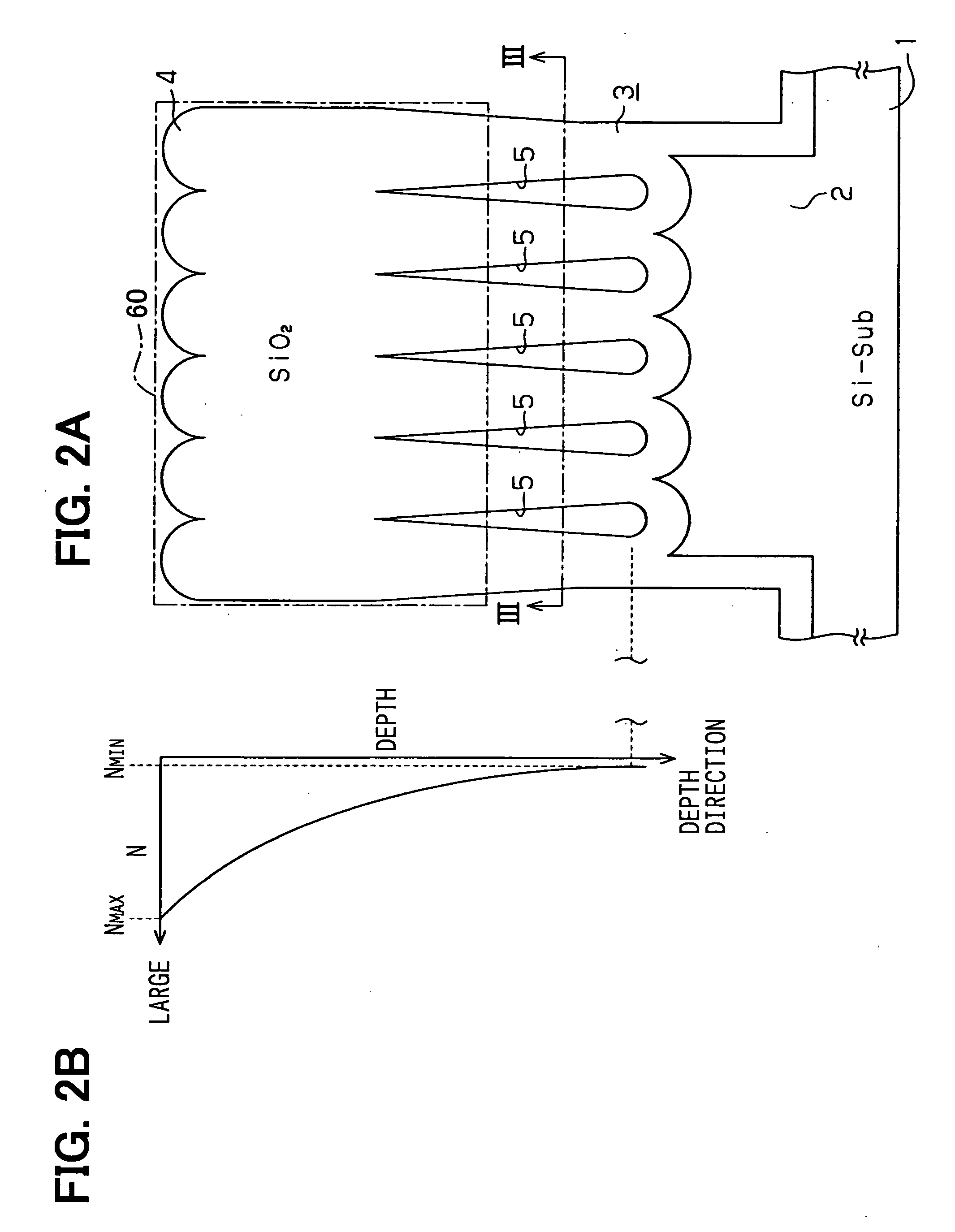
[0055]FIG. 8A shows an optical device having an optical waveguide according to a second embodiment of the present invention. In the device, the trap region 60 as a core layer is not disposed in the upper portion of the optical block 20 but in the middle portion of the block 3 in the vertical direction. Specifically, the block 3 is formed on the base 2 of the substrate 1. Multiple columns 4 are disposed on the substrate 1. Each column 4 has a rectangular plan shape, and is made of silicon oxide. The column 4 has a predetermined height in the vertical direction. The concavity 5 is formed in the lower portion of the block 3, and another cavity 25 as the second cavity is formed in the upper portion of the block 3. The width of the second cavity 25 becomes larger as it goes to the top of the block 3. The width of the cavity 5 becomes larger as it goes to the bottom of the block 3. The width of the second cavity 25 is defined as W4, and the width of the upper portion of the column 4 is de...

third embodiment

[0064]FIG. 13 shows an optical waveguide in an optical device according to a third embodiment of the present invention. In general, the optical waveguide is composed of multiple passages. For example, one passage is divided into multiple passages so that the light wave is divided into multiple light waves. Further, multiple passages are concentrated into one passage so that multiple light waves are concentrated into one light wave.

[0065] In FIG. 13, two light waves are introduced into two inlets of the optical guide, and then, the lights are synthesized into one light wave. Then, the light is outputted from the outlet of the guide. In this case, the first light and the second light are introduced into the first and the second passages 30, 31, and then the light is transmitted in the third passage 32. The width of the first passage 30 is defined as W30, the width of the second passage 31 is defined as W31, and the width of the third passage 32 is defined as W32. Here, the width W30 ...


PUM


Abstract

An optical device includes: a silicon substrate; a plurality of silicon oxide columns having a rectangular plan shape; and a cavity disposed between the columns. Each column has a lower portion disposed on the substrate. Each column has a width defined as W1. The cavity has a width defined as W2. A ratio of W1 / W2 becomes smaller as it goes to the lower portion of the column. A core layer provided by the columns and the cavity can have the thickness equal to or larger than a few dozen μm easily. Therefore, connection loss between a light source and the device is reduced.

Description

CROSS REFERENCE TO RELATED APPLICATION [0001] This application is based on Japanese Patent Application No. 2004-163628 filed on Jun. 1, 2004, the disclosure of which is incorporated herein by reference. FIELD OF THE INVENTION [0002] The present invention relates to an optical device having an optical waveguide and a method for manufacturing an optical device having an optical waveguide. BACKGROUND OF THE INVENTION [0003] An optical waveguide is formed on a substrate such as silicon substrate to have a predetermined shape for transmitting light wave in the waveguide. Therefore, the waveguide is similar to an electric wiring for flowing current. The waveguide is provided by an optical device. The device includes a silicon substrate, a cladding layer on the substrate, and a core layer as an optical waveguide. The core layer is disposed on the substrate through the cladding layer. The cladding layer has low refraction index, and the core layer has high refraction index. [0004] The core ...

Claims


Application Information

Patent Timeline
Patent Type & Authority Applications(United States)
IPC IPC(8): G02B6/122G02B6/13G02B6/136G02B6/26G02B6/42G02B27/00H01L21/311
CPCG02B6/122G02B6/4207G02B6/136
Inventor OOHARA, JUNJIYOSHIHARA, SHINJITAKEUCHI, YUKIHIRO
Owner DENSO CORP
Why Eureka
Try Eureka