Optical waveguide, optical waveguide module and method for forming optical waveguide

a technology of optical waveguides and modules, applied in the field of optical waveguides, can solve problems such as interior arrangement and landscape spoilage, and achieve the effect of reducing connection loss

Inactive Publication Date: 2007-08-09
FURUKAWA ELECTRIC CO LTD
View PDF16 Cites 12 Cited by
  • Summary
  • Abstract
  • Description
  • Claims
  • Application Information

AI Technical Summary

Benefits of technology

[0039] With the optical waveguide of the present invention, the specified portion is bent at the specified radius while reducing connection loss caused by fusion bonding to convert the optical waveguide direction to the specified angle. Further miniaturization of the optical waveguide module is realized using these.

Problems solved by technology

However a principle barrier to increase action speed of the electric circuits is higher than that to increase action speed of optical transmission circuits operational speed.
Further, it is different from necessity of 90 degree direction change of optical waveguide in application region, but for example with FTTH in which optical fibers are wired in users' houses, it is necessary to secure a space for gently bending optical fibers in room corners and hole portions through which the optical fibers pass from outside to inside the house general fibers can not be bent in less than several cms due to problems of mechanical characteristic and optical characteristic, thereby ended up spoiling interior arrangement and landscape.

Method used


Image

  • Optical waveguide, optical waveguide module and method for forming optical waveguide
  • Optical waveguide, optical waveguide module and method for forming optical waveguide
  • Optical waveguide, optical waveguide module and method for forming optical waveguide

Examples


first embodiment

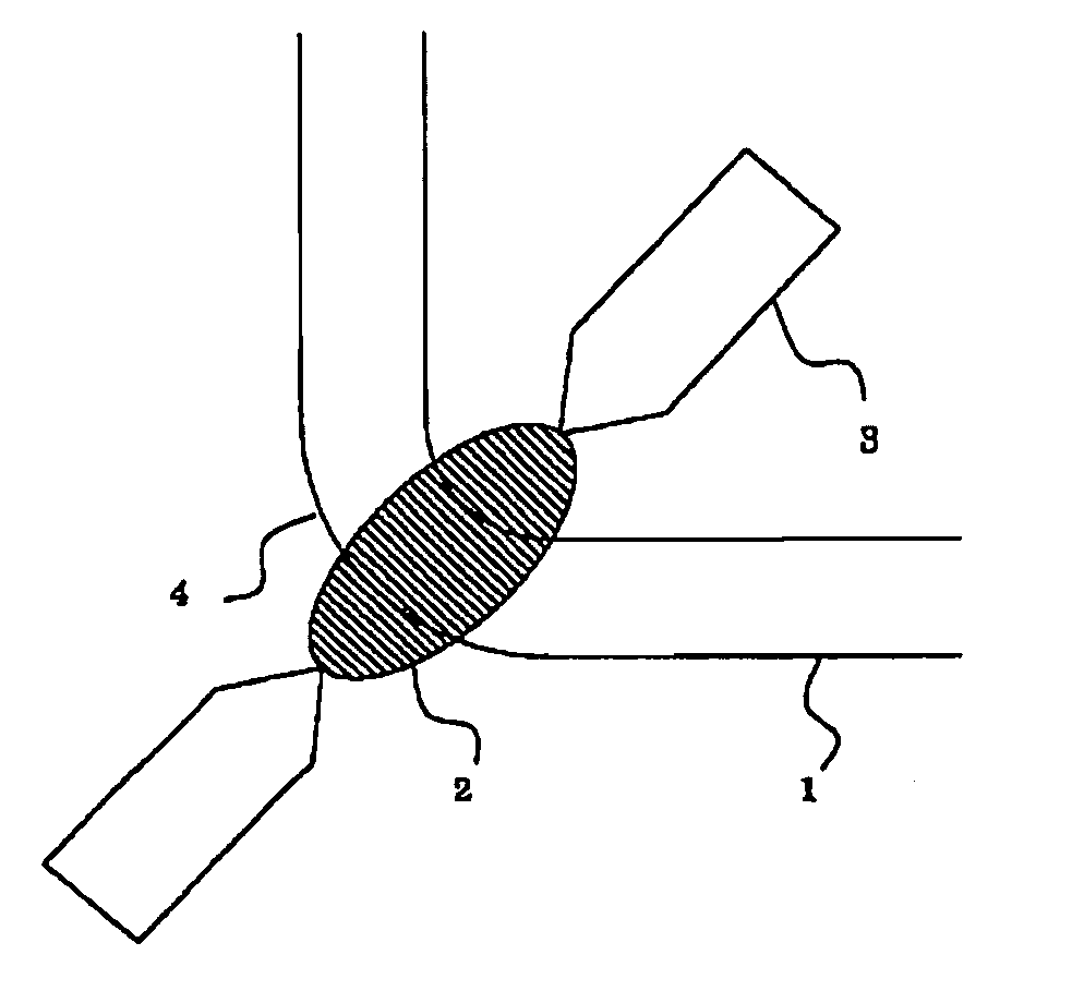
[0060]FIG. 1 is a schematic diagram showing a first mode of an optical waveguide related to the present invention. The specified portion of the optical waveguide is heated by arc discharge to high temperature (more than holding point, less than softening point) and the optical waveguide is bent at a prescribed radius). Since this optical waveguide becomes in a thermoneutral environment after the bent portion of the optical waveguide is bent at high temperature, there is no distortion due to bent. That means it is processed in such that an initial state is a bend state. When the optical waveguide is deformed after processed state, distortion occurs to cause breakage. When the optical waveguide is bent before the process, distortion does not occur to prevent breakage.

[0061] However, when this bent portion is restored to linear state, distortion occurs to cause breakage. Selection whether an initial distortion free state is a linear state or a bent state ends up preventing breakage wh...

second embodiment

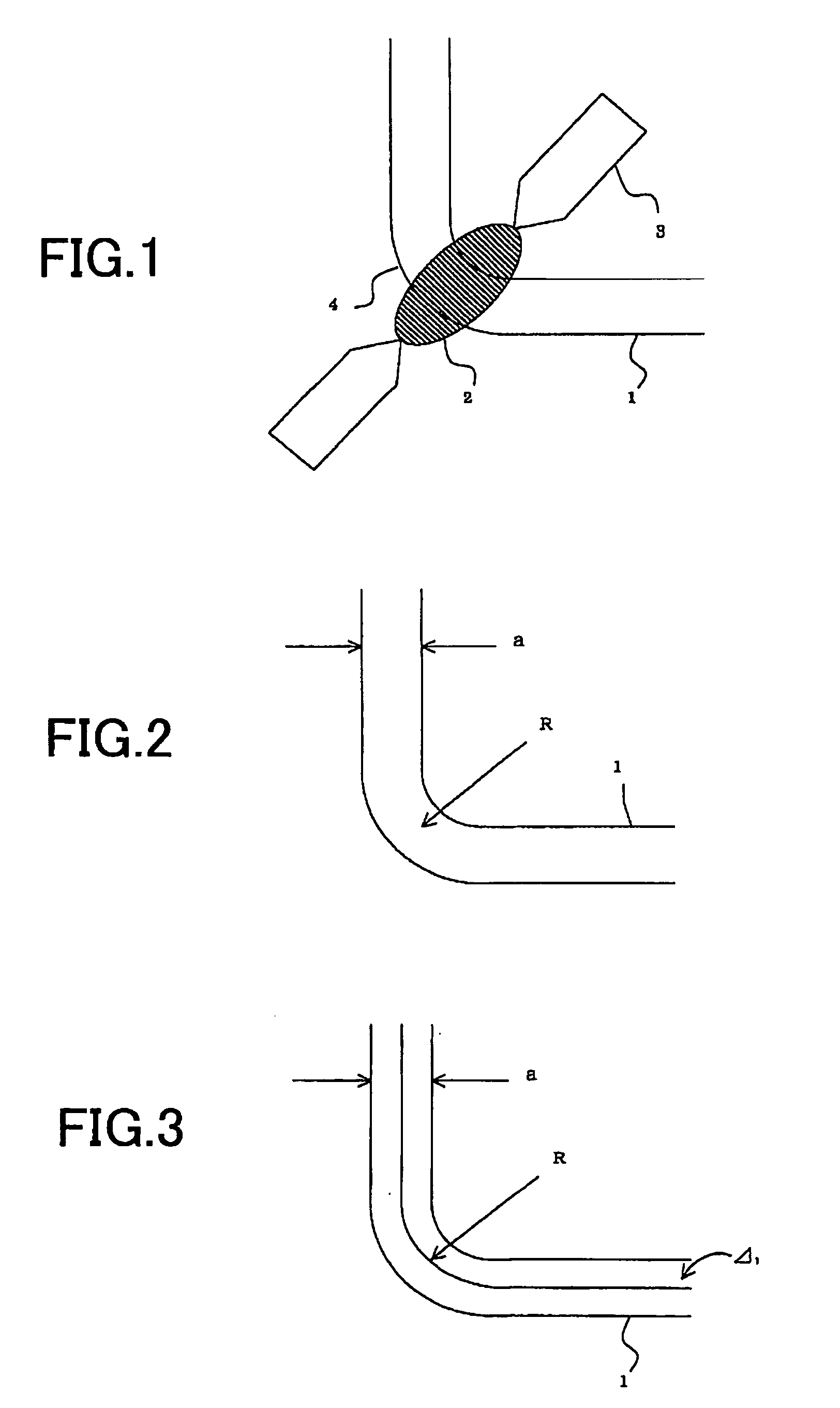
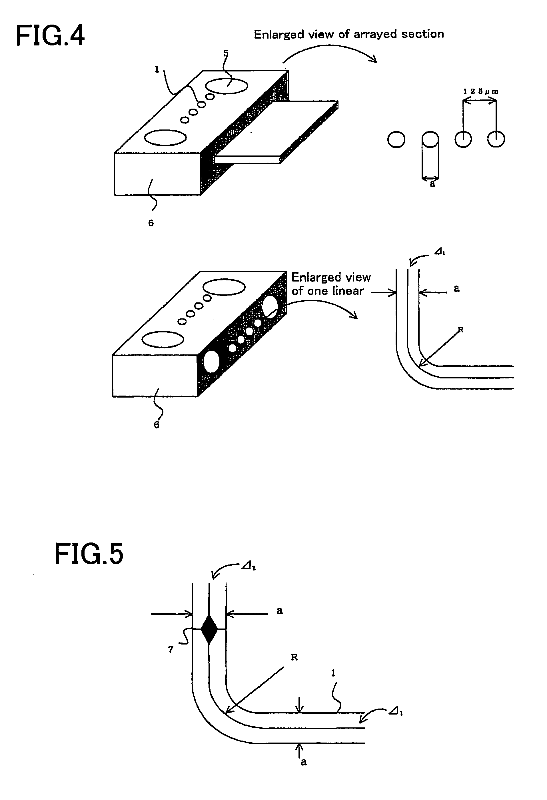
[0063]FIG. 2 is a schematic diagram showing third and fifth modes of an optical waveguide related to the present invention. In these modes where an optical waveguide direction is converted at a minute space, actually usable size is specified based on physical size of the used optical waveguide. In these modes, an external diameter a of the optical waveguide is not less than 50 μm, and a bend radius R is not more than 5.0 mm. That means, it is not physically possible that an optical waveguide with an external diameter a of 50 μm is bent at a bend radius R of 50 μm. It is neither easy to handle an optical waveguide with an external diameter a of less than 50 μm. Therefore, the minimum external diameter a of an optical waveguide is specified 50 μm to secure easy handling and the bend radius of used optical waveguide is specified 10 times of the minimum external diameter to physically realize the bend.

[0064] Further, since 125 μm of external diameter is convertible diameter with the ty...

third embodiment

[0066]FIG. 3 is a schematic diagram showing sixth mode of optical waveguide related to the present invention. A method for preventing mechanical breakage is focused in the optical waveguide direction in the minute space according to the second embodiment. However in this embodiment the optical waveguide direction can be converted in the minute space while maintaining optical characteristics in good condition. An equivalent refractive index difference Δ1 between core and clad of the optical waveguide is within a range from not less than 0.8% to not more than 3.5%, preferably within a range from not less than 1.0% to not more than 3.0%. In the generally used optical waveguide, an general difference Δ1 between the core and the clad is around 0.3%. However, when the optical waveguide having an equivalent refractive index difference Δ1 of about 0.3% is bent at bend radius R of not more than 5.0 mm, light confined in the core is not confined any more and is radiated to the clad, thereby d...


PUM


Abstract

An optical waveguide comprising a core and a clad characterized in that a desired part is heated and transited to machining strain release state, the part transited to the machining strain release state is curved with a specified bending radius and transited to machining strain state. That part of the optical waveguide is heated to a temperature within a range between the bending point and softening point and transited to machining strain state. The optical waveguide is an optical fiber having the outer diameter not shorter than 50 μm. The optical waveguide has the outer diameter not shorter than ten times of the mode field diameter of the optical waveguide. The optical waveguide has a bending radius of 5.0 mm or less and difference equivalent of refractive index &Dgr;1 between the core and clad falls within a range of 0.8-3.5%.

Description

FIELD OF THE INVENTION [0001] The present invention relates to miniaturization of optical components, particularly an optical waveguide, an optical waveguide module which can convert the optical waveguide direction at a minute size and a method for converting an optical waveguide direction. BACKGROUND OF THE INVENTION [0002] Now action speed of electric circuits is approaching that of optical transmission circuits. However a principle barrier to increase action speed of the electric circuits is higher than that to increase action speed of optical transmission circuits operational speed. This is because time constant due to static electric capacity associated with electric circuits increases by the high speed action. Therefore, research and development is actively conducted on fusion of electric circuit and optical circuit to partly compensate a high speed action of electric circuit with an optical transmission path. [0003] Specifically, VCSEL (Vertical Cavity Surface Emitting Laser)...

Claims


Application Information

Patent Timeline
Patent Type & Authority Applications(United States)
IPC IPC(8): G02B6/10G02B6/00G02B6/122G02B6/255
CPCG02B6/2552
Inventor MORIMOTO, MASAHITOSHINODA, MASAO
Owner FURUKAWA ELECTRIC CO LTD
Why Eureka
Try Eureka