Three-dimensional multilayer vertical coupling optical interconnected structure and manufacturing method of soft lithography thereof

A vertical coupling, three-dimensional multi-layer technology, applied in the direction of optical waveguide light guide, light guide, optics, etc., can solve the problems of unsatisfactory connection loss, alignment error scattering loss affecting vertical coupling efficiency, low coupling efficiency, etc., to achieve easy soft light Engraving transfer printing, solving vertical coupling and low connection loss

Inactive Publication Date: 2007-09-12
ZHEJIANG UNIV
View PDF0 Cites 12 Cited by
  • Summary
  • Abstract
  • Description
  • Claims
  • Application Information

AI Technical Summary

Problems solved by technology

It is almost not affected by wavelength changes, but this structure needs to be spin-coated layer by layer. During the process, the alignment error between the layers and the scattering loss caused by the imperfection of the upper layer will affect the vertical Coupling efficiency, and the coupling efficiency is low
[0004] Another solution is to use a silicon substrate, and use mask displacement and reactive ion beam etching to realize an upwardly bifurcated structure, which can etch an S-shaped curved vertical slope that meets various parameters, but requires precise control of air pressure, radio frequency power, and masking. Factors such as the physical size of the mold (including the offset and length of the overhang), and the connection loss is not ideal

Method used


Image

  • Three-dimensional multilayer vertical coupling optical interconnected structure and manufacturing method of soft lithography thereof
  • Three-dimensional multilayer vertical coupling optical interconnected structure and manufacturing method of soft lithography thereof
  • Three-dimensional multilayer vertical coupling optical interconnected structure and manufacturing method of soft lithography thereof

Examples


Embodiment Construction

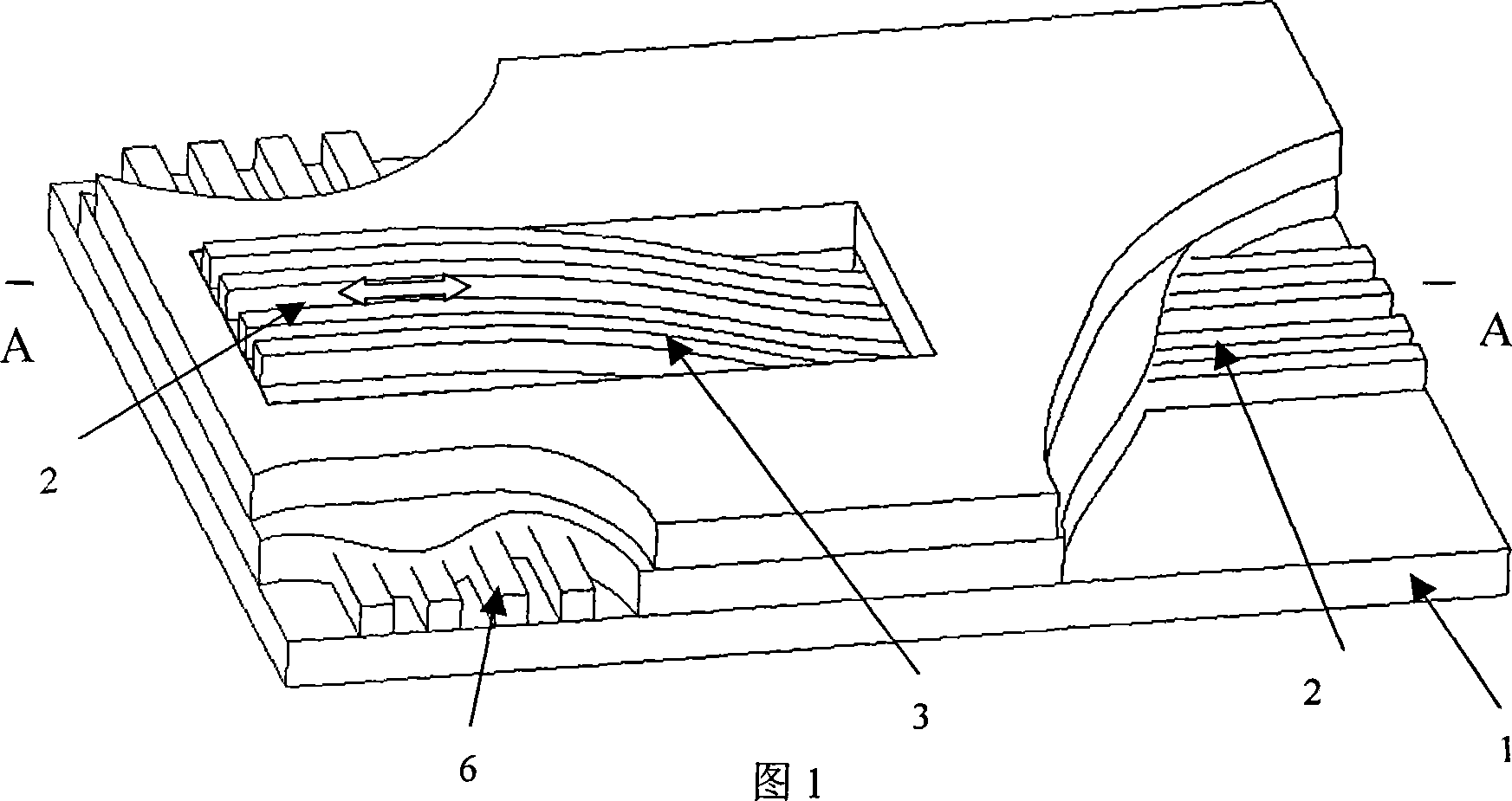
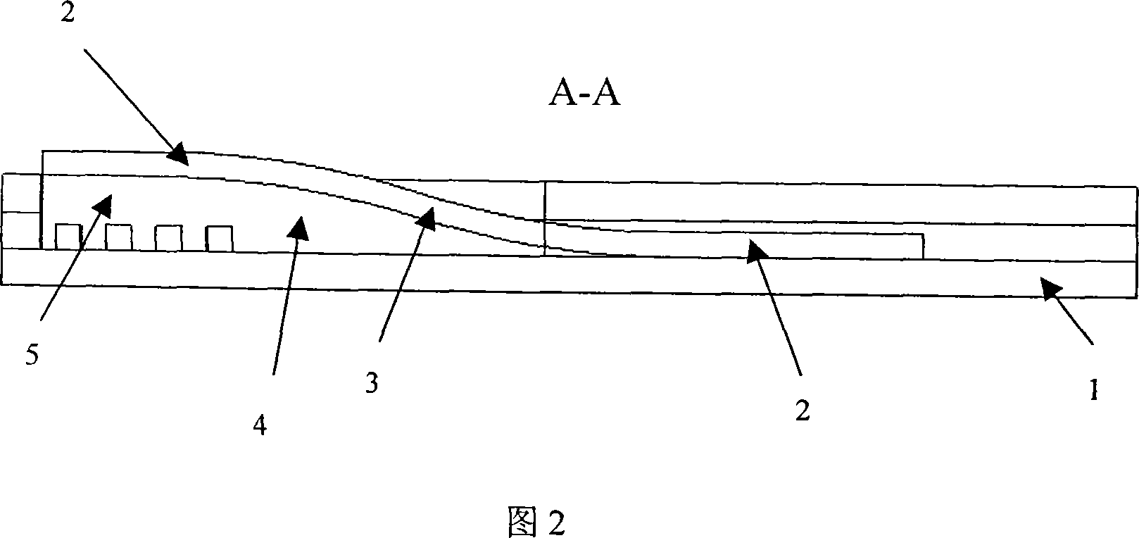
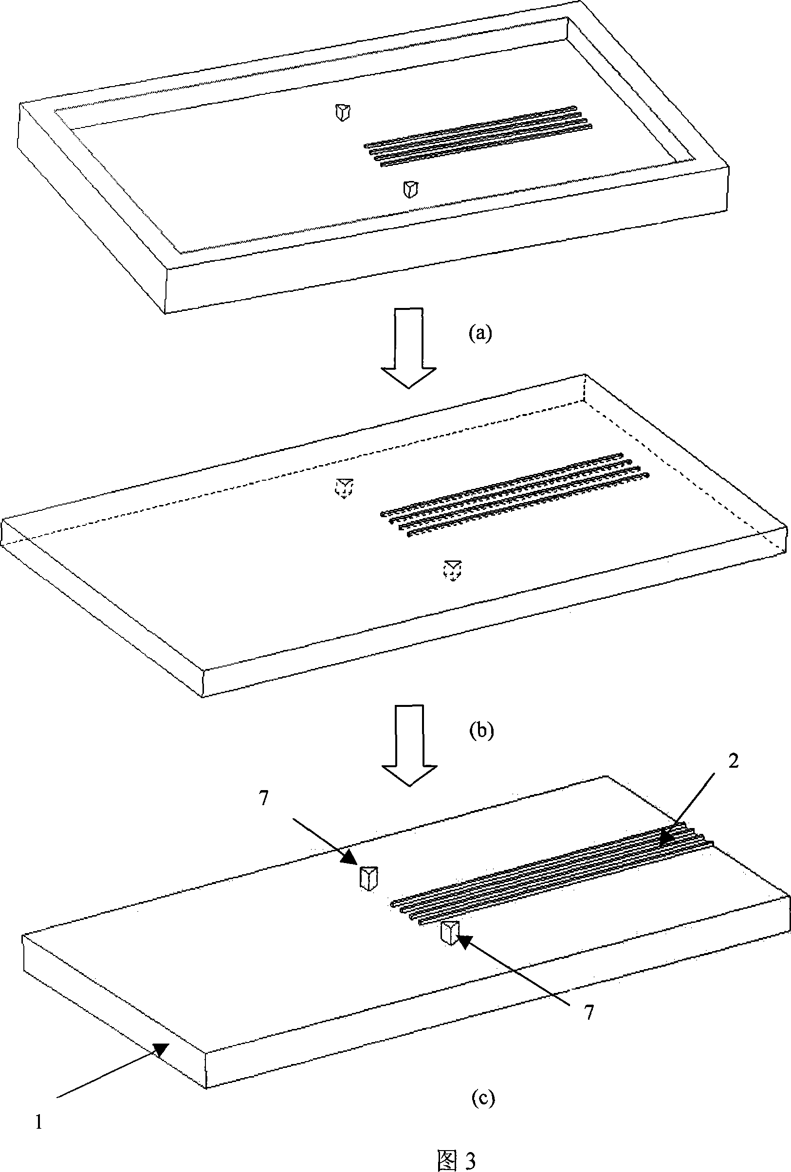
[0019] 1 and 2 are schematic diagrams of a three-dimensional multilayer vertically coupled optical interconnection structure. Including two sets of more than one straight waveguide input and output section 2, S-shaped curved waveguide 3, S-shaped curved slope structure 4, cuboid structure 5, and planar optical transmission waveguide 6; one or more straight waveguide input and output sections 2, S-shaped The curved slope structure 4, the cuboid structure 5 and the planar light transmission waveguide 6 are located on the surface of the substrate 1, the S-shaped curved waveguide 3 is located on the surface of the S-shaped curved slope structure 4, and the input and output section 2 of another or more straight waveguides Located on the surface of the cuboid structure 5, the straight waveguide input and output section 2 on the substrate 1 and the straight waveguide input and output section 2 on the cuboid structure 5 are connected by an S-shaped curved waveguide 3, and the two ends ...


PUM


Abstract

This invention discloses a three diamensions multilayer vertical catenation light interconnecting structure and its photoetching manufacture method. Perpendicular waveguide input and output section, s shape bent slope structure, cuboid structure and plane light transmission waveguide are on the surface of baseplate. S shape bent waveguide is on the surface of s shape bent slope structure. Perpendicular waveguide input and output section if on the surface of cuboid structure. Perpendicular waveguide input and output section that is on the baseplate links that on the cuboid structure by bent waveguide of s shape. Two ends of s shape bent waveguide respectively coaxially link perpendicular waveguide input and output section. The implements vertical multilayer light interconnecting with short span, solves upward or decurrent perpendicular catenation of optical path, makes integrated structure. Alignment error of layers is small. Connection loss is low. The invention is easy to implement photoetching transferring print. The invention can sufficiently display superiority of three diamensions transferring print about high polymer transferring print. The invention is easy to install. Materials are selected from optical high polymer. It has small optical loss and good environment stability.

Description

technical field [0001] The invention relates to a three-dimensional multi-layer vertically coupled optical interconnection structure and a soft photoetching method thereof. Background technique [0002] With the demand for communication capacity and the continuous increase of transmission rate, more and more electronic devices are being replaced by optical devices, no matter in long-distance transmission or short-term communication between integrated circuit chips. Much research has been devoted to the integration of tiny optical devices into planar waveguide devices or photonic integrated circuits (PICs). The role and shape of the photonic integrated circuit PIC are similar to those of a printed circuit board (PCB), but its performance has been greatly improved. PCB provides electronic circuits on one board for connecting various types of electrical devices, such as resistors, diodes, transistors and IC chips, etc., while PIC provides optical circuits for connecting optoel...

Claims


Application Information

Patent Timeline
Patent Type & Authority Applications(China)
IPC IPC(8): G02B6/12G02B6/13G02B6/136
Inventor 倪玮刘彦婷吴兴坤
Owner ZHEJIANG UNIV
Why Eureka
Try Eureka