Method of substrate surface treatment for RRAM thin film deposition

a technology of rram and substrate, applied in the direction of liquid/solution decomposition chemical coating, crystal growth process, polycrystalline material growth, etc., can solve the problems of circuit yield, inability to cover the full circuit area with a single grain of pcmo, and complex device incorporation into state-of-the-art integrated circuit fabrication

Inactive Publication Date: 2005-12-01
XENOGENIC DEV LLC
View PDF4 Cites 12 Cited by
  • Summary
  • Abstract
  • Description
  • Claims
  • Application Information

AI Technical Summary

Problems solved by technology

However, the PCMO must be in crystalline form, which requires that the PCMO must be grown on a specific bottom electrode, such as YBCO, which is not compatible to the state-of-the-art silicon integrated circuit technology.
The growth, or crystallization, temperature is relatively high, e.g., >700° C., which renders incorporation of the device into state-of-the-art integrated circuit fabrication very complex.
In addition it is not possible to cover the full circuit area with a single grain of PCMO.
As the properties of a memory cell which is fabricated on a single grain PCMO crystal and the properties of a memory cell which is fabricated on a multi-grain PCMO crystal, which covers the grain boundary area, are not the same, circuit yield and memory performance problems will occur.

Method used


Image

  • Method of substrate surface treatment for RRAM thin film deposition
  • Method of substrate surface treatment for RRAM thin film deposition
  • Method of substrate surface treatment for RRAM thin film deposition

Examples


Embodiment Construction

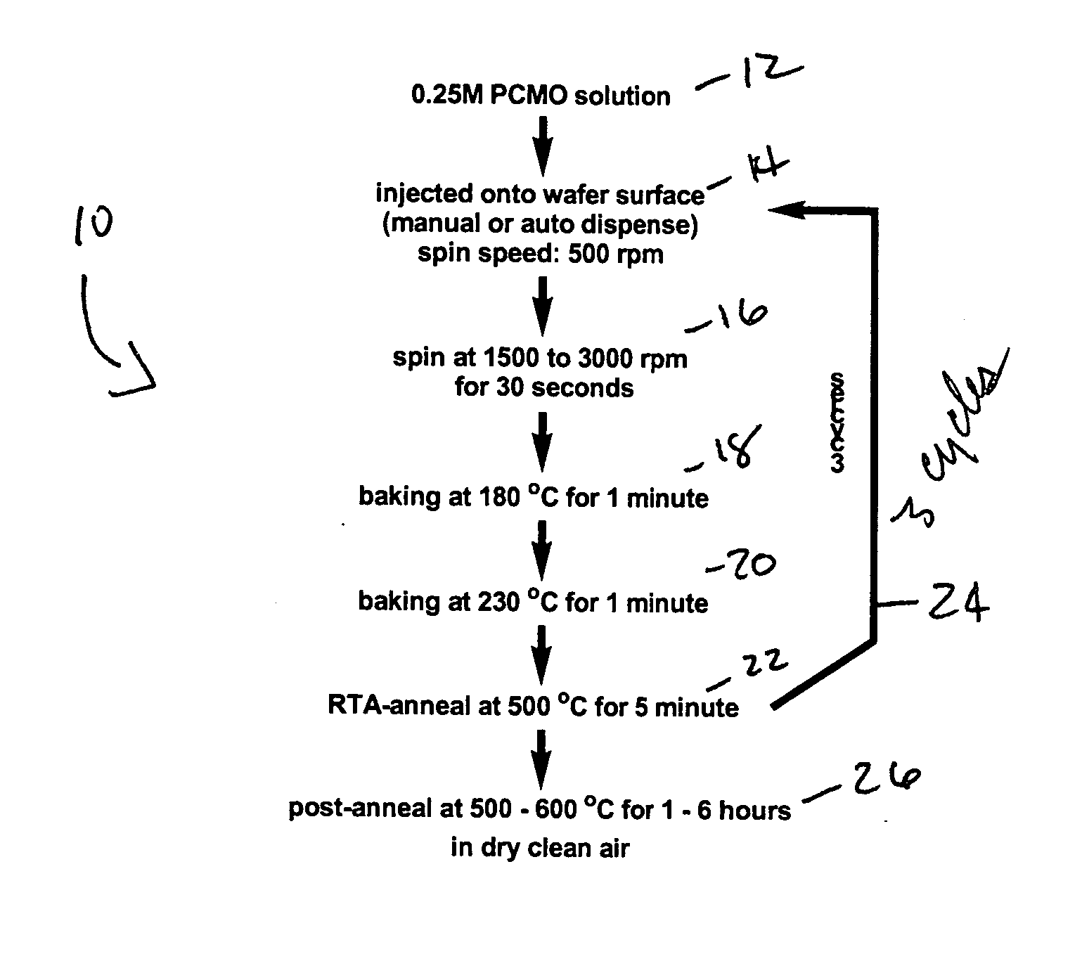
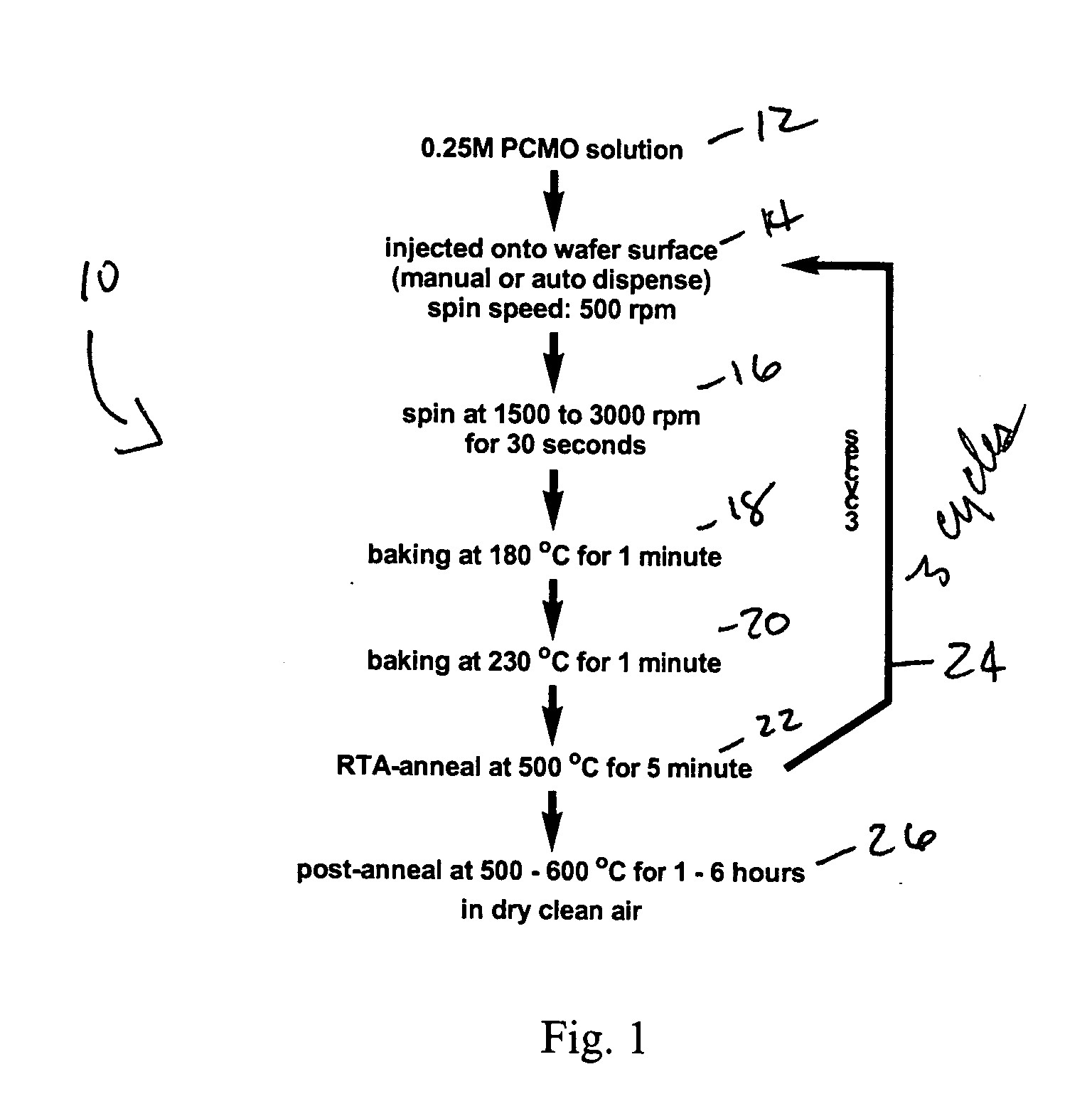
[0014] Transition metals, after a special surface treatment of the method of the invention, may be used as electrodes for the integration of RRAM thin film. Colossal magnetoresistive (CMR) material, such as Pr0.3Ca0.7MnO3 (PCMO), exhibit resistive switching properties upon application of an electrical pulse. The first example of the method of the invention includes fabrication of a PCMO thin film deposited on a substrate of rhodium, surface-treated with an alloy of Pt0.2Co0.8. The film demonstrates reversible resistant changes with the application of narrow electric pulses.

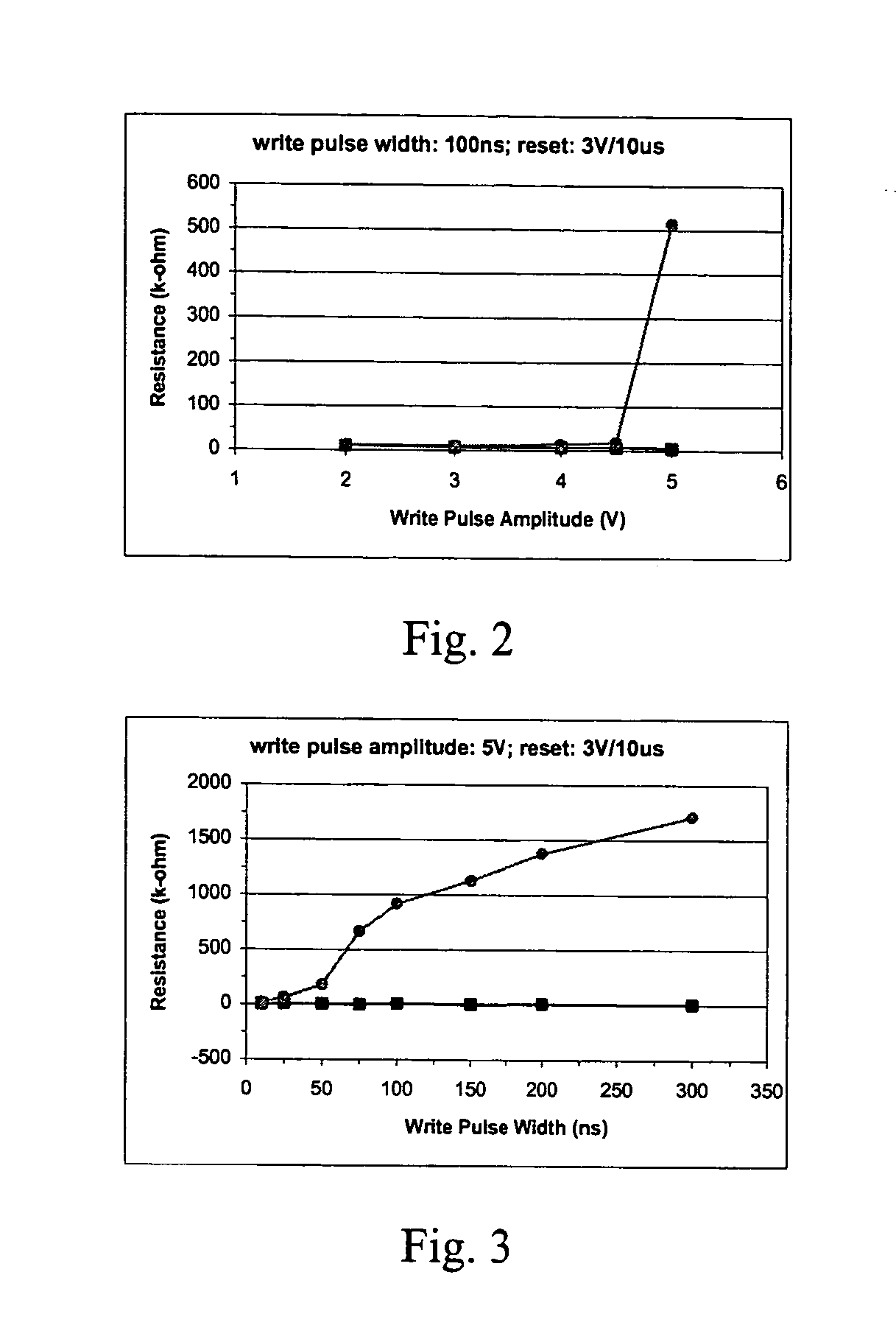
[0015] PCMO thin films have been found to have reversible resistance change properties. The resistance may be increased to a high resistance state by applying an electric pulse of nanosecond duration, such as 5V electrical amplitude and 100 ns pulse duration time. To reset the resistance to a low resistant state, a microsecond electric pulse, e.g., a 3V amplitude and 10 μs pulse width, may be applied. This unique...


PUM

PropertyMeasurementUnit
temperatureaaaaaaaaaa

Abstract

A method of fabricating a CMR thin film for use in a semiconductor device includes preparing a CMR precursor in the form of a metal acetate based acetic acid solution; preparing a wafer; placing a wafer in a spin-coating chamber; spin-coating and heating the wafer according to the following: injecting the CMR precursor into a spin-coating chamber and onto the surface of the wafer in the spin-coating chamber; accelerating the wafer to a spin speed of between about 1500 RPM to 3000 RPM for about 30 seconds; baking the wafer at a temperature of about 180° C. for about one minute; ramping the temperature to about 230° C.; baking the wafer for about one minute at the ramped temperature; annealing the wafer at about 500° C. for about five minutes; repeating said spin-coating and heating steps at least three times; post-annealing the wafer at between about 500° C. to 600° C. for between about one to six hours in dry, clean air; and completing the semiconductor device.

Description

FIELD OF THE INVENTION [0001] This invention relates to fabrication of RRAM devices, and specifically to the use of surface-treated transition metals as the substrate for RRAM thin film deposition, which surface-treated transition metals provide the thin films with reversible resistance change properties. BACKGROUND OF THE INVENTION [0002] Perovskite metal oxide thin films, such as Pr0.3Ca0.7MnO3 (PCMO), exhibit reversible resistance change when an electric pulse is applied. A PCMO thin film has been grown on both epitaxial YBa2Cu3O7 (YBCO) and partial epitaxial Pt substrates via pulsed laser abrasion (PLA) technique, Liu et al., Electric-pulse-induced reversible resistance change effect in magnetoresistive films, Applied Physics Letters, 76, 2749, 2000; and Liu et al., U.S. Pat. No. 6,204,139, granted Mar. 20, 2001, for Method of switching the properties of perovskite materials used in thin film resistors. which describes the resistance change which occurred when electric pulses ar...

Claims


Application Information

Patent Timeline
Patent Type & Authority Applications(United States)
IPC IPC(8): C23C18/12C30B23/02C30B29/24H01L21/44H01L45/00
CPCC23C18/1216C23C18/1225C23C18/1241C23C18/1283C30B23/02H01L45/147H01L45/1253H01L45/1608H01L45/04H01L45/1233C30B29/24H10N70/20H10N70/841H10N70/8836H10N70/021H10N70/826
Inventor ZHUANG, WEI-WEILI, TINGKAIPAN, WEIEVANS, DAVID R.HSU, SHENG TENG
Owner XENOGENIC DEV LLC
Why Eureka
Try Eureka