Semiconductor equipment having multiple semiconductor devices and multiple lead frames

a technology of semiconductor devices and lead frames, which is applied in the direction of semiconductor devices, semiconductor/solid-state device details, electrical apparatus, etc., can solve the problems of increasing the manufacturing cost of equipment, and the temperature increase of the chip b>124/b> is not desirable, and achieves the effect of not increasing the temperature of the second device and high accuracy

Active Publication Date: 2005-12-08
DENSO CORP
View PDF3 Cites 19 Cited by
  • Summary
  • Abstract
  • Description
  • Claims
  • Application Information

AI Technical Summary

Benefits of technology

[0008] In the above equipment, the temperature of the first semiconductor device is prevented from transmitting to the second device. Thus, the temperature of the second device is not increased. Accordingly, the equipment has high accuracy without operational failure.

Problems solved by technology

This causes to increase manufacturing cost of the equipment.
Further, the temperature increase of the chip 124 is not desirable.

Method used


Image

  • Semiconductor equipment having multiple semiconductor devices and multiple lead frames
  • Semiconductor equipment having multiple semiconductor devices and multiple lead frames
  • Semiconductor equipment having multiple semiconductor devices and multiple lead frames

Examples


first embodiment

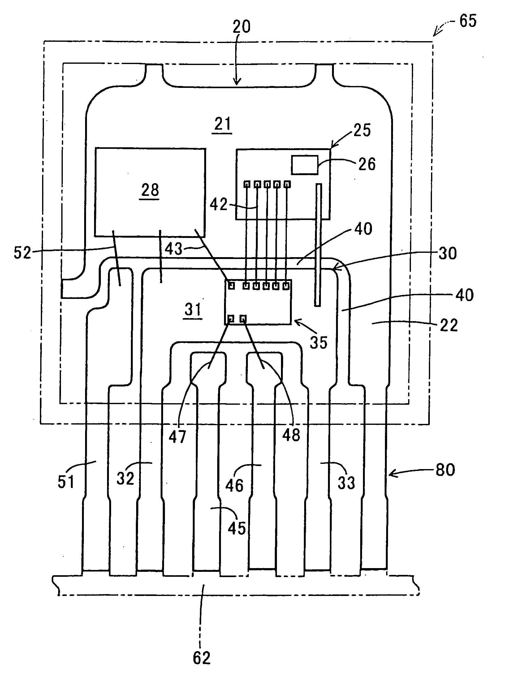
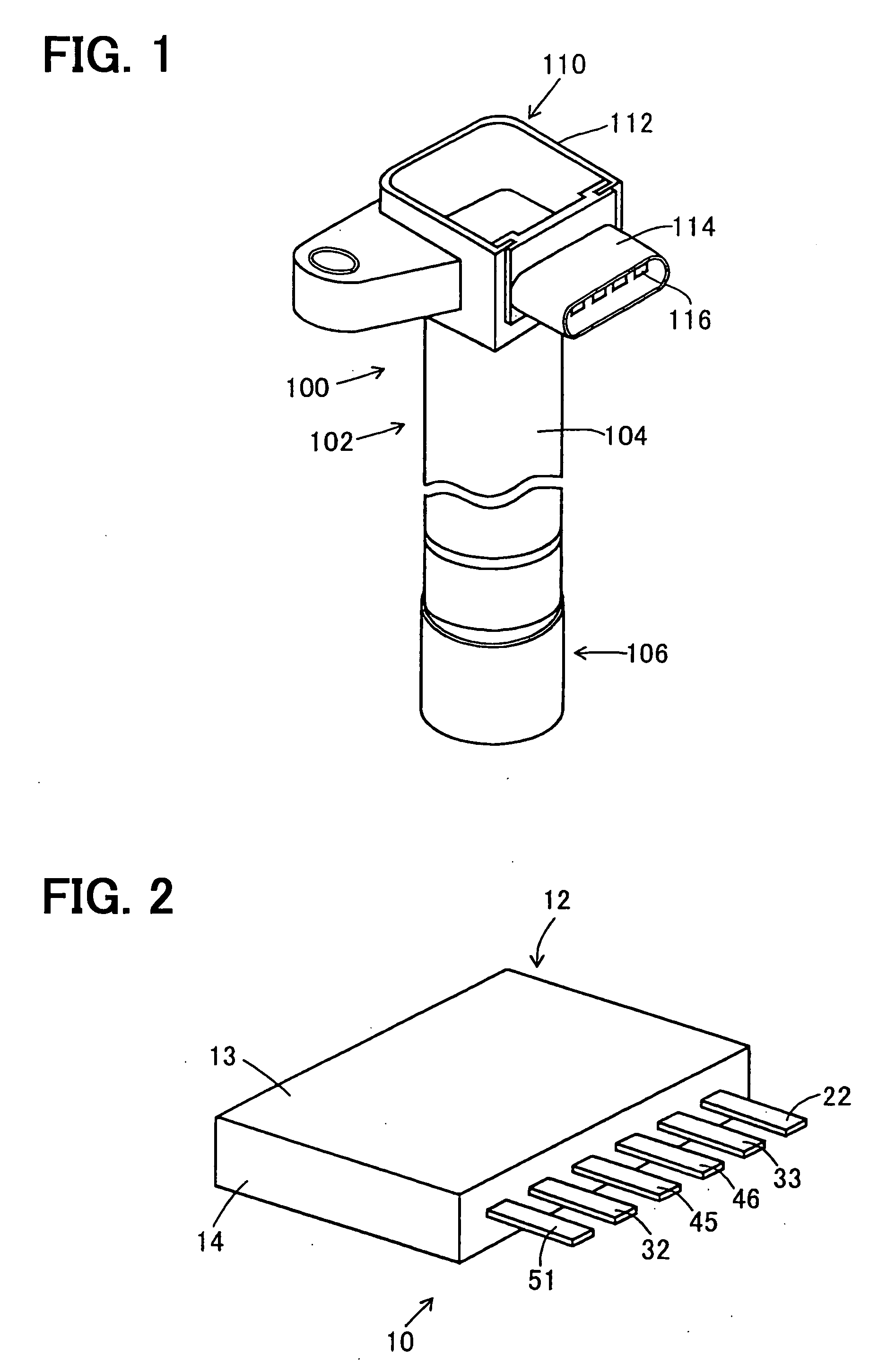
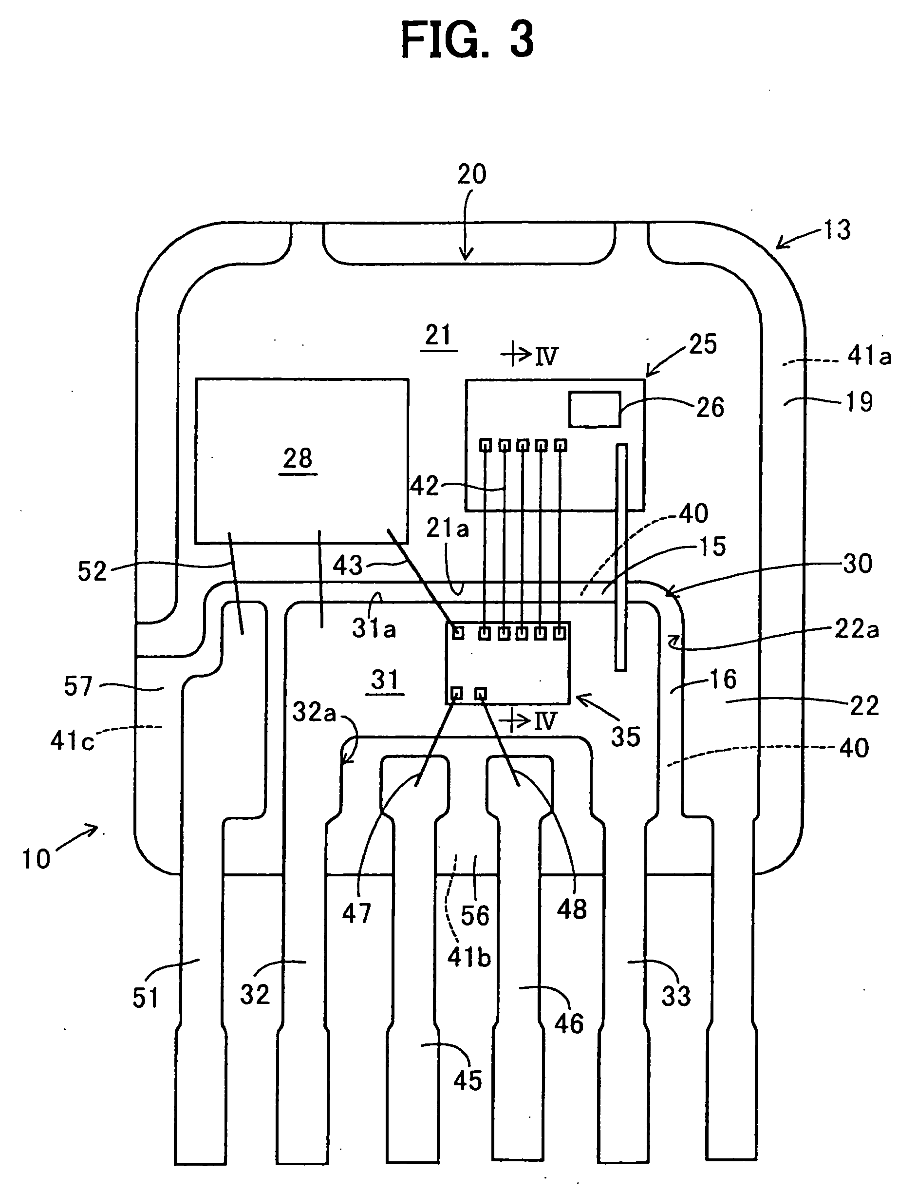
[0021] Semiconductor equipment according to a first embodiment of the present invention is shown in FIG. 1. The equipment is suitably used for an igniter for switching the primary current of the primary coil on and off. The igniter is mounted on an ignition coil of an automotive vehicle (i.e., a stick coil). As shown in FIG. 1, the stick coil 100 is composed of a coil portion 102, a tower portion 106 and a controller 110. The coil portion 102 is disposed in a middle of the coil 100 in a longitudinal direction. The tower portion 106 is disposed below the coil portion 102. The controller 110 is disposed above the coil portion 102. The coil portion 102 accommodates the primary coil and a secondary coil (not shown) inside a body casing 104. The controller 110 accommodates an igniter 10 for switching the primary current of the primary coil on and off. Specifically, the igniter 10 is disposed in an upper casing 112. An external terminal 116 is disposed on a connector 114.

[0022] The ignit...

second embodiment

[0039]FIGS. 8A and 8B show a method for manufacturing semiconductor equipment according to a second embodiment of the present invention. The assembly 80 is accommodated in an upper casing 70. Specifically, the assembly 80 is positioned in the upper casing 70 before the assembly 80 is not molded with resin. Then, epoxy resin is inserted into the upper casing 70 so that the epoxy resin covers the casing 70. Specifically, as shown in FIG. 8A, the assembly 80 is mounted in a concavity 73 of a base 72, which protrudes from a sidewall 71 of the upper casing 70. The base 72 protrudes inside of the casing 70. Then, the first extension part 22 of the first lead frame 20, the second extension part 33 of the second lead frame 30, and the third, the fourth and the fifth lead frames 45, 46, 51 are connected to a terminal 76 of a connector 75 through a bonding wire 77.

[0040] After that, the first extension part 22, the second extension part 33 and the like are removed from the connection portion...


PUM


Abstract

Semiconductor equipment includes: a first lead frame having a first semiconductor device; a second lead frame having a second semiconductor device; a thermal resistor for preventing heat transfer from the first lead frame to the second lead frame; and a temperature sensitive device for detecting operational temperature of the first semiconductor device. The first lead frame is separated from the second lead frame by a predetermined distance. The thermal resistor is disposed in a clearance between the first lead frame and the second lead frame. The second semiconductor device controls to restrict operation of the first semiconductor device when the operational temperature of the first semiconductor device is higher than a predetermined temperature.

Description

CROSS REFERENCE TO RELATED APPLICATIONS [0001] This application is based on Japanese Patent Applications No. 2004-165946 filed on Jun. 3, 2004, and No. 2005-112512 filed on Apr. 8, 2005, the disclosures of which are incorporated herein by references. FIELD OF THE INVENTION [0002] The present invention relates to semiconductor equipment having multiple semiconductor devices and multiple lead frames. BACKGROUND OF THE INVENTION [0003] Some kind of semiconductor equipment has a power device and a control device disposed on a lead frame. The control device controls the power device. The power device, the control device and the lead frame are molded with resin. Here, the temperature of the power device is easily increased when the power device is operated. Therefore, it is preferred that the equipment includes heat radiation means for preventing operation failure when the temperature of the power device is increased. This type of equipment is disclosed in, for example, Japanese Patent Ap...

Claims


Application Information

Patent Timeline
Patent Type & Authority Applications(United States)
IPC IPC(8): H01L23/34H01L23/495
CPCH01L23/34H01L2924/19107H01L23/49575H01L24/49H01L2224/48091H01L2224/48137H01L2224/48247H01L2224/4903H01L2224/49051H01L2224/49171H01L2224/49175H01L2924/01004H01L2924/01005H01L2924/01006H01L2924/01029H01L2924/01082H01L2924/13055H01L2924/14H01L2924/19043H01L23/49562H01L2924/01033H01L24/48H01L2924/00014H01L2924/00H01L2924/00012H01L2924/181H01L2224/05554H01L2924/10161H01L2224/45099
Inventor KAWAKITA, HARUOANDO, KOJI
Owner DENSO CORP
Why Eureka
Try Eureka