Optical path switching device

Inactive Publication Date: 2005-12-08
SHARP KK
View PDF1 Cites 0 Cited by
  • Summary
  • Abstract
  • Description
  • Claims
  • Application Information

AI Technical Summary

Benefits of technology

[0038] With this method, it is possible to efficiently manufacture an optical pat

Problems solved by technology

In some cases, however, only a reduction in the entire thickness does not effectively lower a driving voltage.
As a result, the electrical field intensity is relatively reduced for the same voltage, and an appropriate electro-optic effect for the light that passes through the device cannot be obtained.
First, the crystal material portion 301 is partially made very thin; therefore, it becomes difficult to form a position reference for the assembly of the optical path switching device itself.
In addition, the formation of the position reference on a plane that is not parallel to this optical path easily makes the position reference unclear.
Furthermore, in some cases, the thickness of this crystal material portion becomes extremely thin; therefore, the electro-optic effect of the crystal material portion, i.e., an important portion of the optical path switching device, is negatively affected to a great

Method used


Image

  • Optical path switching device
  • Optical path switching device
  • Optical path switching device

Examples


Example

Embodiment 1

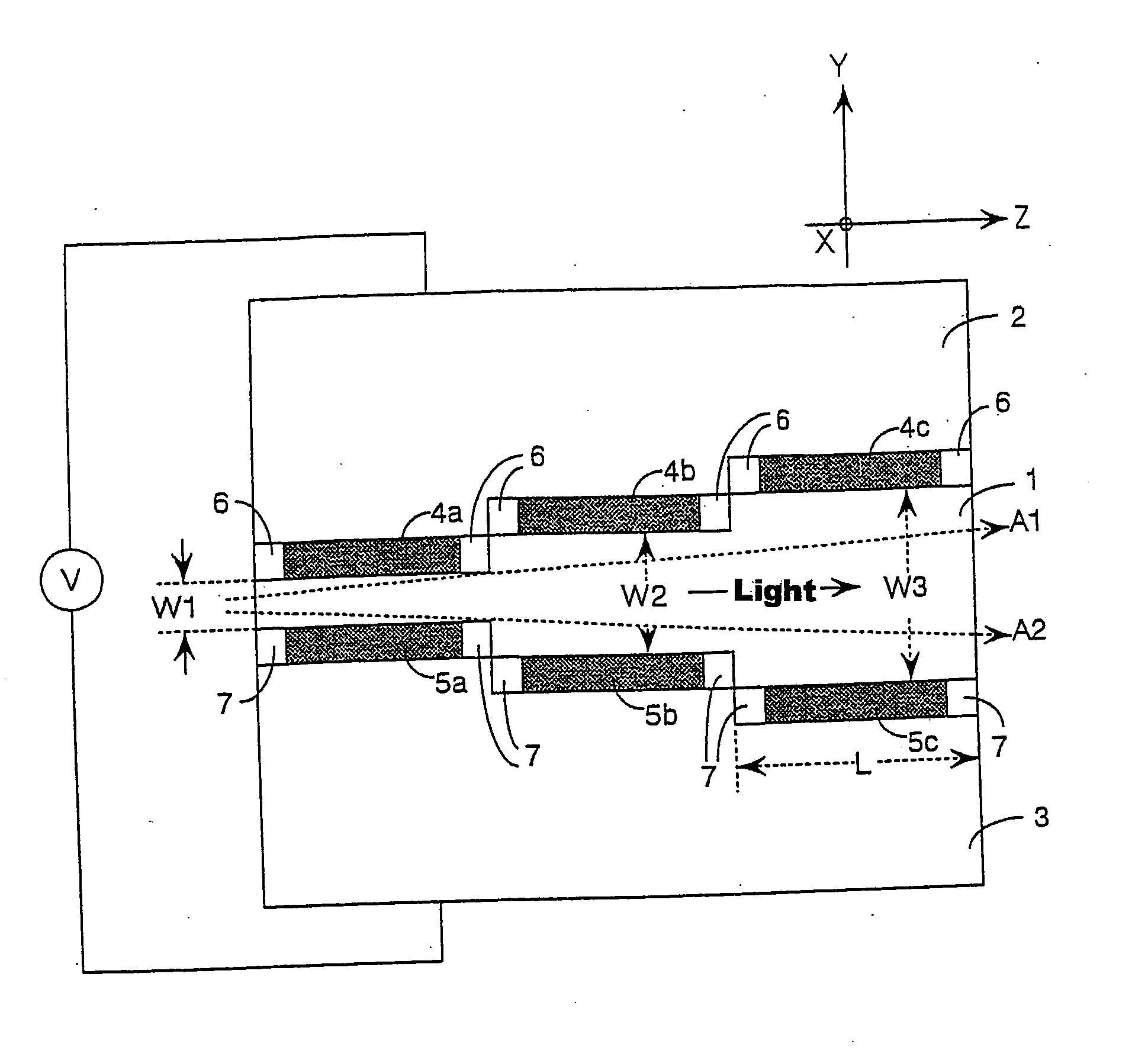
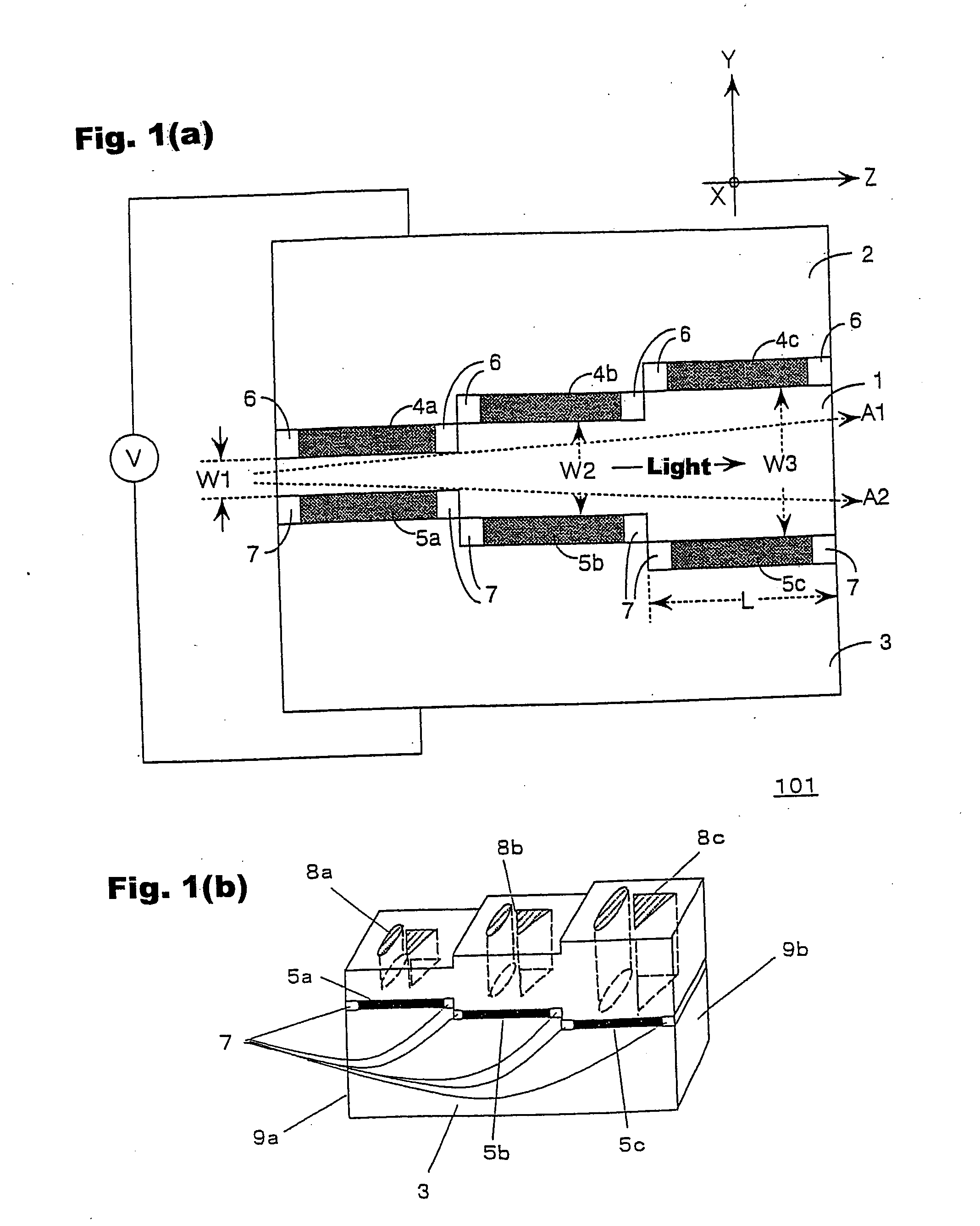
[0055] First, one embodiment of the present invention will be described with reference to FIGS. 1(a) and 1(b). FIG. 1(a) is a side diagram of an optical path switching device 101, and FIG. 1(b) is a perspective diagram showing a portion of the optical path switching device 101 that is below a crystal material portion 1.

[0056] In FIG. 1(a), the optical path switching device 101 of the present invention is formed of the crystal material portion 1, a first support member 2, a second support member 3, first electrode layers 4a, 4b and 4c, second electrode layers 5a, 5b and 5c, first adhesive layers 6 and second adhesive layers 7. In the case where the first support member 2 and the second support member 3 are made of a conductive material, a voltage V for modulating a refractive index is applied between the upper surface of the first support member 2 and the lower surface of the second support member 3.

[0057] The crystal material portion 1 is formed in a manner where the ...

Example

Embodiment 2

[0110] FIGS. 7(a) and 7(b) are diagrams showing the structure of an optical path switching device according to Embodiment 2 of the present invention.

[0111]FIG. 7(a) is a cross sectional diagram of the optical path switching device as viewed from the side, and FIG. 7(b) is a perspective diagram of the optical path switching device, from which the first support member 22, which is the upper portion of the device, has been removed.

[0112] The optical path switching device 102 of Embodiment 2 is formed of a crystal material portion 21, a first support member 22, a second support member 23, a first electrode layer 24, second electrode layers 25 (25a, 25b and 25c), first adhesive layers 26 and second adhesive layers 27.

[0113] In Embodiment 2, only the surfaces on one side of the crystal material portion 21 are in step form, and the thickness varies in the structure. The surface on the other side is a flat surface having no steps. In addition, as shown in FIG. 7(b), refracti...

Example

Embodiment 3

[0129] An optical path switching device where the thickness of the crystal material portion from the entrance side to the emission side varies in so-called taper form will be described below.

[0130] FIGS. 9(a) and 9(b) are a cross sectional diagram of the optical path switching device of Embodiment 3 and a perspective diagram showing a portion of the device from which the first support member 32 has been removed.

[0131] In FIG. 9(a), the length of the crystal material portion 31 on the entrance surface 39c side in the direction from the top to the bottom in the plane of the paper is 70 μm, the length of the crystal material portion 31 on the emission surface 39d side in the direction from the top to the bottom in the plane of the paper is 200 μm, and the surfaces of the crystal material portion 31 that face the first support member 32 and the second support member 33 are both formed as flat surfaces.

[0132] In addition, refractive region groups 38 which are the same as ...


PUM


Abstract

An optical path switching device comprises a light transmitting portion, a first electrode layer, a second electrode layer, a first adhesive layer, a second adhesive layer, a first supporting portion and a second supporting portion. The light transmitting portion has a plurality of refracting regions wherein the refractive indexes of a light can be uniformly controlled by the electro-optic effect in the direction perpendicular to the traveling direction of the light, and the thickness of the light transmitting portion changes along the traveling direction of the light. The first electrode layer and the second electrode layer are so formed as to sandwich the light transmitting portion and as to cover at least a part of the refracting regions. The first supporting portion is tightly arranged on a side of the first electrode layer, which side is out of contact with the light transmitting layer, via the first adhesive layer. The second supporting portion is tightly arranged on a side of the second electrode layer, which side is out of contact with the light transmitting layer, via the second adhesive layer.

Description

TECHNICAL FIELD [0001] The present invention relates to an optical path switching element, and relates to an electrical field modulation-type optical path switching element which uses a bulk-type electro-optic crystal to electrically implement a lens effect. BACKGROUND ART [0002] There is a technique for modulating a refractive index by an electro-optic effect so as to switch an optical path. A device for obtaining a lens effect by an electro-optic effect disclosed in Patent Document 1 (Japanese Unexamined Patent Application No. Hei 1(1989)-230017) will be described below with reference to FIGS. 13 and 14. [0003] The device of FIG. 13 has a configuration that an electro-optic medium (crystal material portion) 301 is placed between electrodes 302 and a voltage applied from a voltage power supply 303 is changed so that a change in refractive index is caused. Herein, the lens effect is obtained by forming each of the electrodes 302 into a shape capable of obtaining the lens effect, as ...

Claims


Application Information

Patent Timeline
IPC IPC(8): G02F1/29G02B6/12G02F1/03
CPCG02F1/0316G02F1/29G02F2201/16
Inventor MINAMI, KOHJI
Owner SHARP KK
Why Eureka
Try Eureka