Wafer processing method

a processing method and a technology of a wafer, applied in the direction of laser beam welding apparatus, manufacturing tools, semiconductor devices, etc., can solve the problems of destroying the semiconductor chips, causing fatal damage to the semiconductor chips, and unable to cut the above low-k film at the same time, so as to prevent the influence of debris

Active Publication Date: 2005-12-15
DISCO CORP
View PDF11 Cites 58 Cited by
  • Summary
  • Abstract
  • Description
  • Claims
  • Application Information

AI Technical Summary

Benefits of technology

[0010] It is an object of the present invention to provide a wafer processing method capable of preventing the influence of debris produced by the application of a laser beam along streets formed on a wafer.

Problems solved by technology

It is difficult to cut the above Low-k film and test element group (TEG) at the same time with the cutting blade because they are formed of a material different from that of the wafer.
That is, as the Low-k film is extremely fragile like mica, a problem occurs in that when the above semiconductor wafer is cut along the streets with the cutting blade, the Low-k film peels off, and this peeling reaches the circuits and causes a fatal damage to the semiconductor chips.
Also, since the test element group (TEG) is formed of a metal, problems occur in that when the semiconductor wafer having the test element group (TEG) is cut with the cutting blade, a burr is produced and the service life of the cutting blade is shortened.
This scattered debris accumulate in an unprocessed area right before processing, and accumulated debris block the laser beam applied.
As a result, there arises a problem that the Low-k film in the unprocessed area and the test element group (TEG) formed on the streets cannot be removed surely.
Furthermore, even when a laser beam is applied along the streets formed on the wafer to divide it into individual chips, the laser beam is blocked by the debris accumulated in the above unprocessed area and hence, the energy of the laser beam is not fully absorbed into the processing point of the wafer.
Therefore, there is a problem that the wafer cannot be divided into individual chips.

Method used


Image

  • Wafer processing method
  • Wafer processing method
  • Wafer processing method

Examples


Embodiment Construction

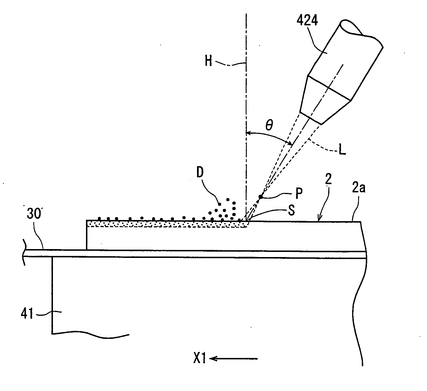
[0044] A wafer processing method according to the present invention of the present invention will be described in detail hereinunder with reference to the accompanying drawings.

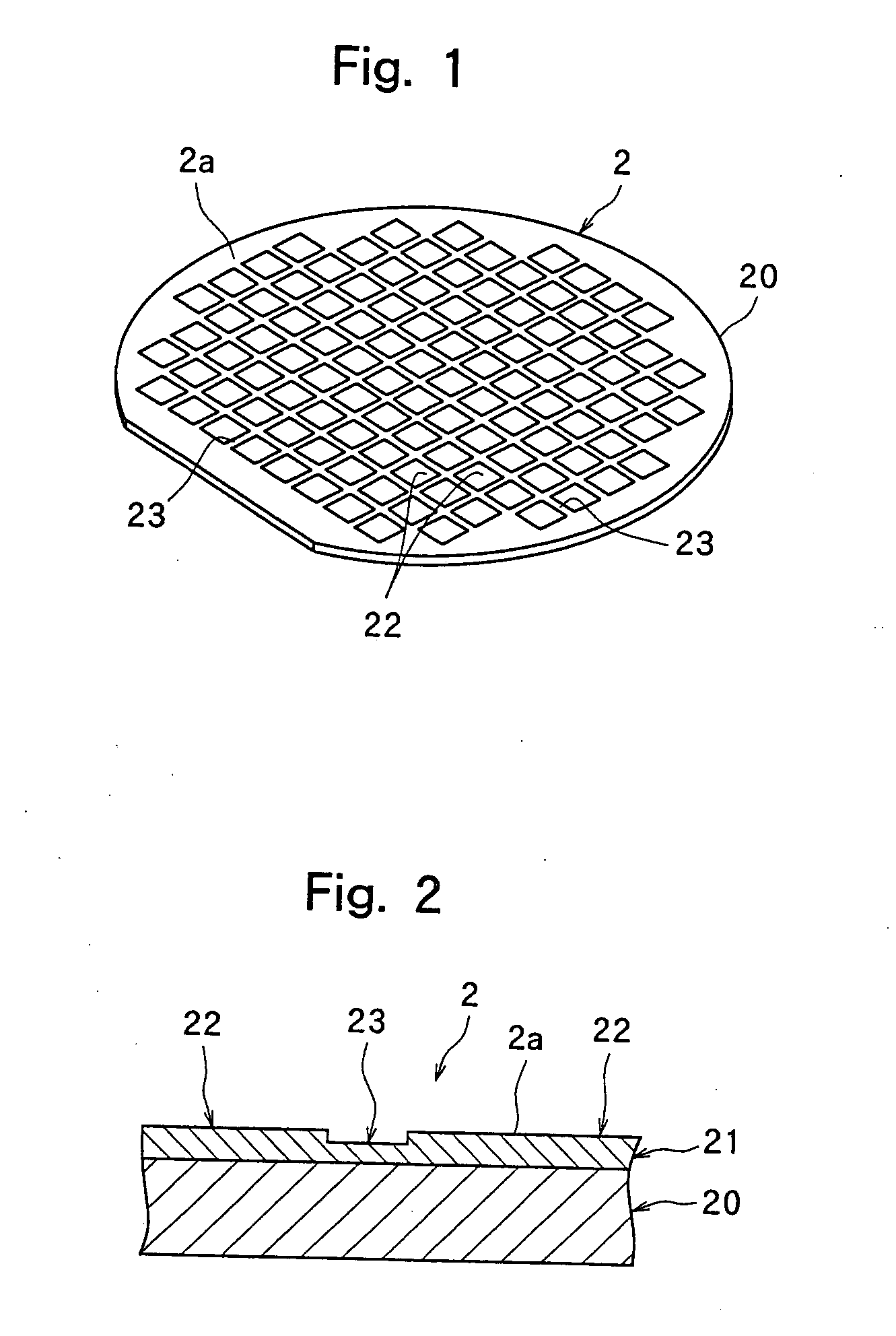
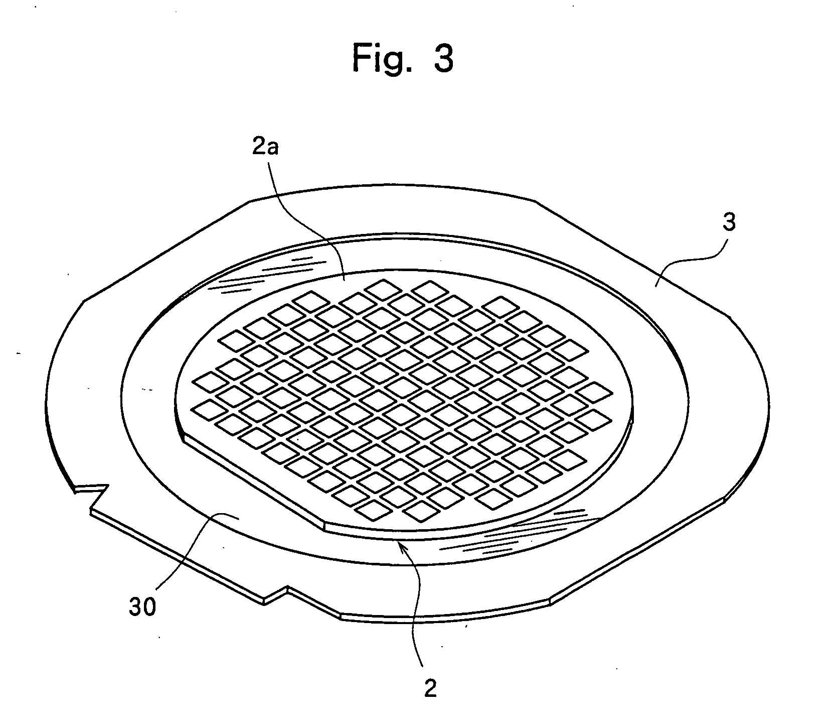
[0045]FIG. 1 is a perspective view of a semiconductor wafer as a workpiece to be processed by the wafer processing method of the present invention, and FIG. 2 is an enlarged sectional view of the principal section of the semiconductor wafer shown in FIG. 1. In the semiconductor wafer 2 shown in FIG. 1 and FIG. 2, a plurality of semiconductor chips 22 such as IC's or LSI's composed of a laminate 21 consisting of an insulating film and a functional film forming circuits are formed in a matrix on the front surface 20a of a semiconductor substrate 20 such as a silicon substrate. The semiconductor chips 22 are sectioned by streets 23 formed in a lattice pattern. In the illustrated embodiment, the insulating film forming the laminate 21 is an SiO2 film or a low-dielectric insulating film (Low-k film) formed of a f...


PUM

PropertyMeasurementUnit
incident angleaaaaaaaaaa
diameteraaaaaaaaaa
diameteraaaaaaaaaa

Abstract

A wafer processing method for carrying out processing by applying a laser beam along streets formed on a wafer, comprising a step of applying a laser beam at an incident angle of a predetermined inclination angle to the normal line of a processing surface of the wafer while the wafer is processing-fed along a street from one end to the other end on the side of the laser beam application at an acute angle to the processing surface of the wafer.

Description

FIELD OF THE INVENTION [0001] The present invention relates to a wafer processing method for carrying out processing by applying a laser beam along streets formed on a wafer such as a semiconductor wafer or an optical device wafer. DESCRIPTION OF THE PRIOR ART [0002] As is known to people of ordinary skill in the art, a semiconductor wafer having a plurality of semiconductor chips such as IC's or LSI's, which are formed in a matrix on the front surface of a semiconductor substrate such as a silicon substrate and composed of a laminate consisting of an insulating film and a functional film, is formed in the production process of a semiconductor device. In the semiconductor wafer thus formed, the above semiconductor chips are sectioned by dividing lines called “streets”, and individual semiconductor chips are manufactured by cutting the semiconductor wafer along the streets. An optical device wafer having optical devices comprising gallium nitride-based compound semiconductors in a pl...

Claims


Application Information

Patent Timeline
Patent Type & Authority Applications(United States)
IPC IPC(8): B23K26/08B23K26/16B23K26/18B23K26/364B23K101/40H01L21/301H01L21/78
CPCB23K26/16H01L33/0095H01L21/78
Inventor YOSHIKAWA, TOSHIYUKITSUCHIYA, TOSHIO
Owner DISCO CORP
Why Eureka
Try Eureka