Method and system for inspecting a wafer

a wafer and inspection method technology, applied in the field of methods for inspecting wafers, can solve the problem that structures derive from previous process steps cannot have an interfering

Inactive Publication Date: 2005-12-22
VISTEC SEMICON SYST
View PDF9 Cites 28 Cited by
  • Summary
  • Abstract
  • Description
  • Claims
  • Application Information

AI Technical Summary

Benefits of technology

[0020] According to the present invention, a wafer inspection system for inspecting a wafer, in particular for examining edge bead removal, is equipped with an optical detector for acquiring an optical image of the region to be inspected, and with a data readout device for reading out the image data furnished by the optical detector, having a computer unit connected to the data readout device for comparing acquired images of the region to be inspected. It is sufficient and advantageous if the system comprises a single optical detector that acquires a first image prior to application of a layer onto the wafer, and a second image af

Problems solved by technology

As a result, structures that derive from previous pr

Method used


Image

  • Method and system for inspecting a wafer
  • Method and system for inspecting a wafer
  • Method and system for inspecting a wafer

Examples


Embodiment Construction

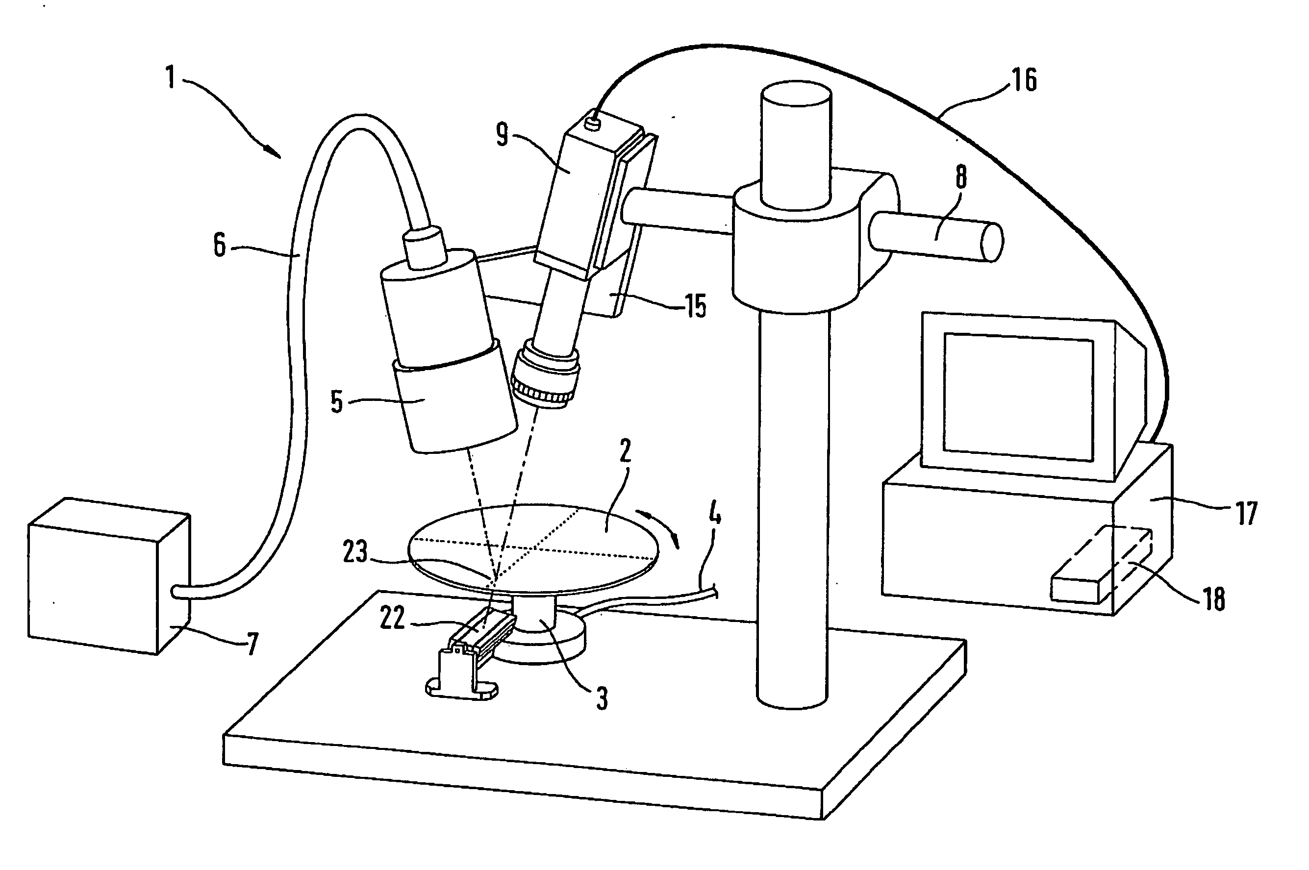
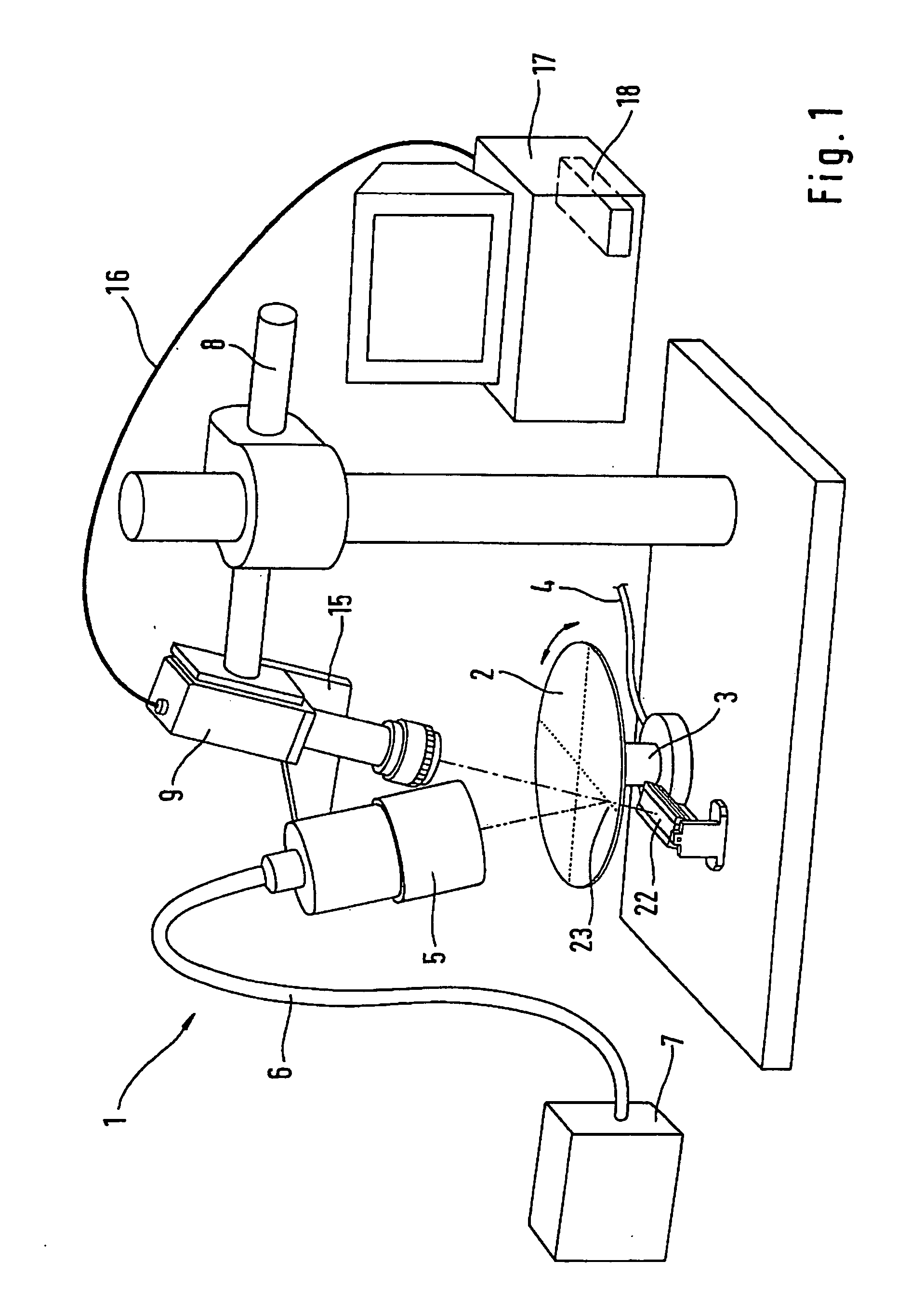
[0033]FIG. 1 shows a system for wafer inspection, in particular for examining edge bead removal, that is suitable for the present invention. An optical detector 9, in this case an imaging device in the form of a CCD linear camera, and an incident illumination device 5 are directed onto a region to be inspected of wafer 2 in the region of its wafer edge 23. The overall system for wafer inspection is labeled 1. A wafer edge position detection device 22 is provided for alignment of the wafer, an alignment being performed by means of illumination beneath wafer 2. The image data acquired by imaging device 9 are transferred via a data line 16 to a data readout device 17. This data readout device 17 is or contains a computer unit 18 for evaluating acquired images.

[0034] System 1 depicted here makes possible incident illumination in both bright- and dark-field modes. For that purpose, incident illumination device 5 is directed onto the region to be inspected of wafer edge 23 of wafer 2. Li...


PUM


Abstract

A method for inspecting a wafer includes acquiring, prior to an application of a layer onto the wafer, a first optical image of a region of the wafer surface to be inspected. After at least partial removal of the layer, a second optical image is acquired. The region of the wafer surface is inspected by comparing the first and the second images.

Description

CROSS REFERENCE TO RELATED APPLICATIONS [0001] Priority is claimed to German patent application 10 2004 029 012.1, the entire disclosure of which is hereby incorporated by reference herein. FIELD OF THE INVENTION [0002] The invention concerns a method for inspecting a wafer, in particular for examining edge bead removal, an optical image of the region to be inspected being acquired. The invention further concerns a corresponding system having an optical detector for acquiring an optical image of the region to be inspected. Lastly, the invention concerns a computer program and a computer program product for implementing the inspection method. BACKGROUND OF THE INVENTION [0003] In semiconductor production, wafers are coated with layers such as photoresist and often also anti-reflection layers. This is generally done by applying a predetermined amount of the substance to be applied onto the rotating wafer disk, on which the substance becomes uniformly distributed. With this method, sli...

Claims


Application Information

Patent Timeline
IPC IPC(8): G01N21/88G01N21/95G01N21/956G06T5/00G06T5/50G06T7/00H01L21/66
CPCG01N21/9503G06T2207/30148G06T7/001G01N2021/8825
Inventor BACKHAUSS, HENNINGKREH, ALBERT
Owner VISTEC SEMICON SYST
Why Eureka
Try Eureka