Method of removing a sacrificial emitter feature in a BICMOS process with a super self-aligned BJT

a technology of bicmos and self-alignment, applied in the field of semiconductor processing, can solve the problems of complex, time-consuming, and expensive techniques, and achieve the effect of facilitating the complete removal of the mask layer

Inactive Publication Date: 2005-11-08
MAXIM INTEGRATED PROD INC
View PDF6 Cites 5 Cited by
  • Summary
  • Abstract
  • Description
  • Claims
  • Application Information

AI Technical Summary

Benefits of technology

[0006]In general, the invention relates to a method of removing a sacrificial emitter feature in a bipolar complementary metal oxide semiconductor (BICMOS) process with a super self-aligned bipolar junction transistor (BJT). According to the new method, a mask layer, such as an oxide deposited using high density plasma (HDP) techniques, is deposited over an extrinsic base layer and over a sacrificial emitter structure. Because of particular characteristic of this mask layer, the deposition of this mask layer forms a triangular-like structure over the sacrificial emitter structure having a maximum thickness less than the thickness of the mask layer over the extrinsic base layer. This facilitates the complete removal of the mask layer above the sacrificial emitter layer without the complete removal of the mask layer above the extrinsic base layer. This allows the removal of the sacrificial emitter structure while the mask layer protects the underlying extrinsic base layer.

Problems solved by technology

Such techniques are rather expensive, time-consuming, and complex.

Method used


Image

  • Method of removing a sacrificial emitter feature in a BICMOS process with a super self-aligned BJT
  • Method of removing a sacrificial emitter feature in a BICMOS process with a super self-aligned BJT
  • Method of removing a sacrificial emitter feature in a BICMOS process with a super self-aligned BJT

Examples


Embodiment Construction

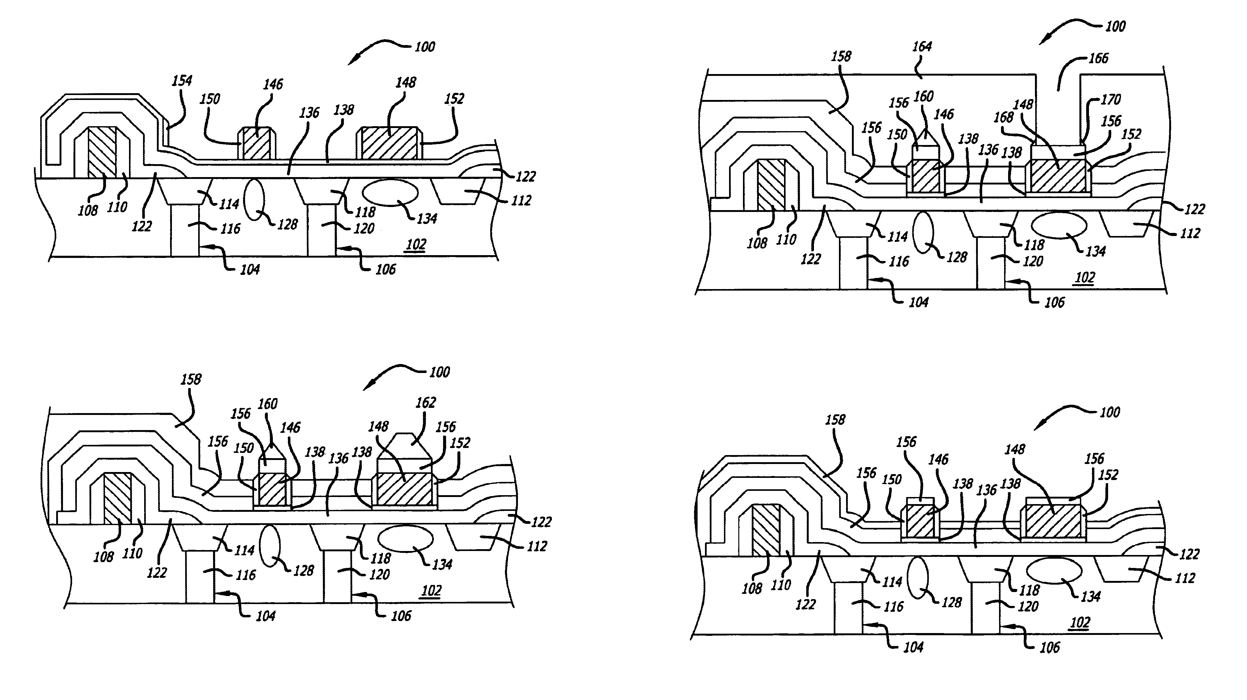
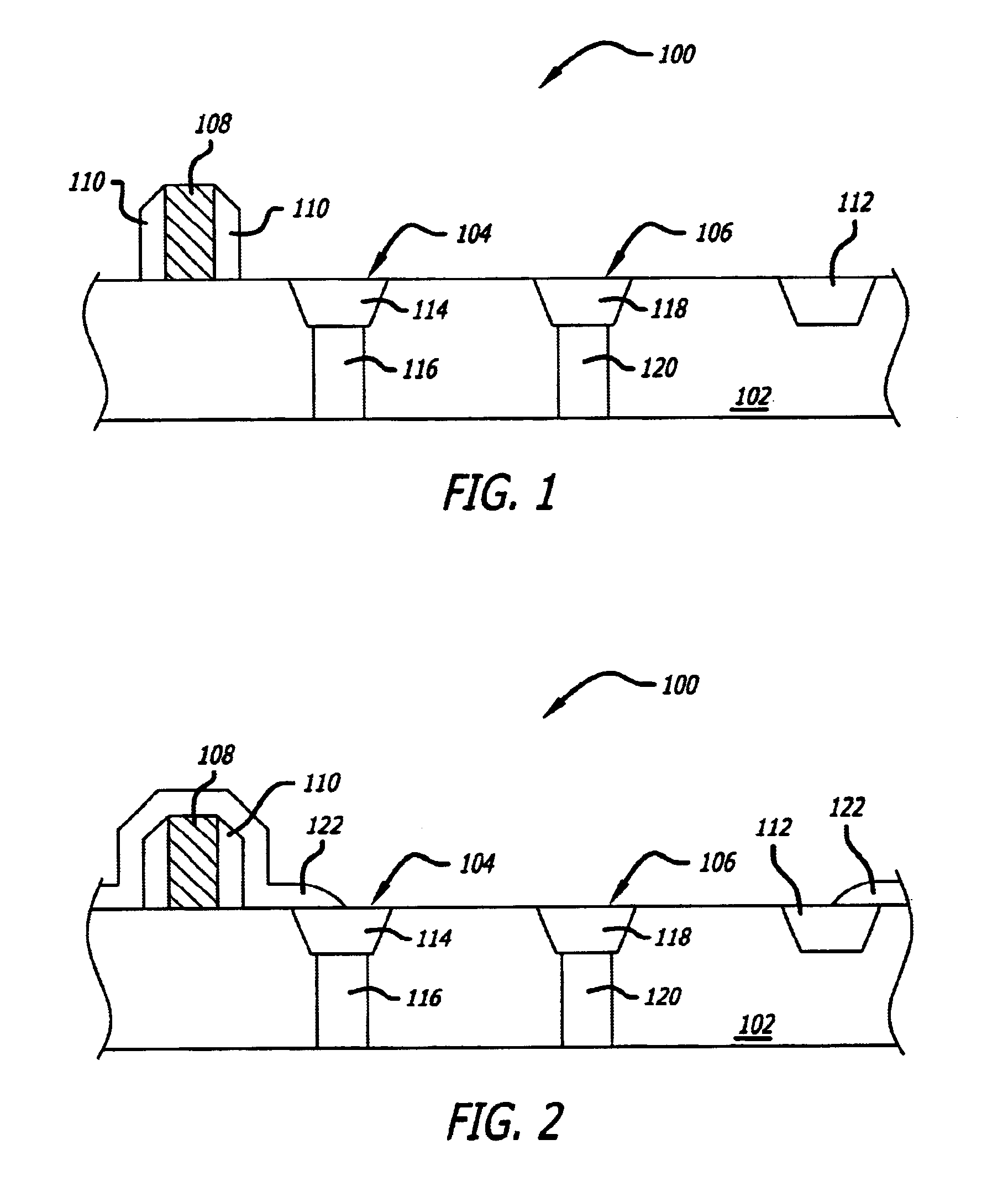
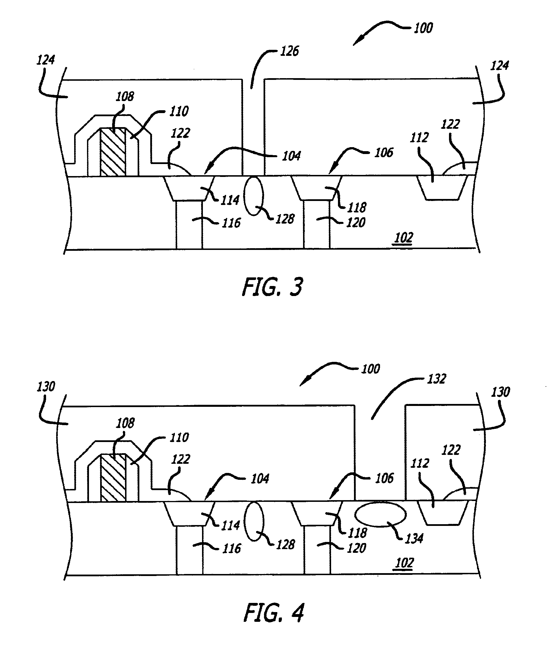
[0012]FIG. 1 illustrates a cross-sectional view of a semiconductor device 100 at an intermediate stage of a method of removing a sacrificial emitter feature in a BICMOS process with a super self-aligned BJT in accordance with an embodiment of the invention. At this stage, the semiconductor device 100 comprises a substrate 102, first and second isolation structures, such as shallow and deep trench isolation structures 104 and 106, a doped polycrystalline silicon (“polysilicon”) gate 108 with spacer 110 on its sidewall, and a stand-alone isolation structure, such as shallow trench isolation structure 112. The shallow and deep trench isolation structures 104 and 106 respectively comprise shallow trench portions 114 and 118 formed near the surface of the substrate 102, and deep trench portions 116 and 120 formed within the substrate respectively below the shallow trench portions 114 and 118. In this example, the thickness of the polysilicon gate is about 2000 to 2500 angstroms.

[0013]FIG...


PUM


Abstract

A method of removing a sacrificial emitter feature in a bipolar complementary metal oxide semiconductor (BICMOS) process with a super self-aligned bipolar junction transistor (BJT) is disclosed. According to the new method, a mask layer, such as an oxide deposited using high density plasma (HDP) techniques, is deposited over an extrinsic base layer and over a sacrificial emitter structure. Because of the particular characteristic of the HDP oxide, the deposition of HDP oxide forms a triangular-like structure over the sacrificial emitter structure having a maximum thickness less than the thickness of the HDP oxide over the extrinsic base layer. This facilitates the complete removal of the HDP oxide above the sacrificial emitter layer without the complete removal of the HDP oxide above the extrinsic base layer. This allows the removal of the sacrificial emitter structure while the remaining HDP oxide, serving as a mask, protects the underlying extrinsic base layer.

Description

FIELD OF THE INVENTION[0001]This invention relates generally to semiconductor processing, and in particular, to a method of removing a sacrificial emitter feature in a bipolar complementary metal oxide semiconductor (BICMOS) process with a super self-aligned bipolar junction transistor (BJT).BACKGROUND OF THE INVENTION[0002]Bipolar junction transistors (BJTs) are commonly formed in integrated circuits along side with complementary metal oxide semiconductor (CMOS) devices. Such simultaneous manufacturing of these two different types of devices is sometimes referred to in the relevant art as a BICMOS process. In a BICMOS process, one or more isolation structures are typically formed within a substrate to electrically isolate the bipolar device from the CMOS device. Once the isolation structures are formed, the BICMOS process continues to complete the manufacturing of the CMOS and bipolar devices.[0003]With regard to the manufacturing of the BJT device, typically the process entails fo...

Claims


Application Information

Patent Timeline
Patent Type & Authority Patents(United States)
IPC IPC(8): H01L21/70H01L29/00H01L21/8238H01L21/331H01L21/8249
CPCH01L21/8249H01L29/66287
Inventor KALNITSKY, ALEXANDERPARK, SANG H.ZEKERIYA, VIKTORWANG, LARRY
Owner MAXIM INTEGRATED PROD INC
Why Eureka
Try Eureka