Drive circuit for display apparatus and plasma display apparatus

a drive circuit and display apparatus technology, applied in the direction of instruments, filing appliances, pulse techniques, etc., can solve the problems of output device cu or output device lu being destroyed, and achieve the effect of preventing output device from being destroyed and avoiding malfunctions

Inactive Publication Date: 2006-01-05
FUJITSU HITACHI PLASMA DISPLAY LTD
View PDF13 Cites 10 Cited by
  • Summary
  • Abstract
  • Description
  • Claims
  • Application Information

AI Technical Summary

Benefits of technology

[0018] The first object of the present invention is to prevent output devices from being destroyed by avoiding malfunctions when the power is turned on.
[0019] The second object of the present invention is to make it possible to prevent ...

Problems solved by technology

In the case where the circuit shown in FIG. 2 is used in the sustain circuit shown in FIG. 5, when the power of the circuit is turned on, the output voltage HO is fixed to the “high (H)” level and an abnormal curr...

Method used


Image

  • Drive circuit for display apparatus and plasma display apparatus
  • Drive circuit for display apparatus and plasma display apparatus
  • Drive circuit for display apparatus and plasma display apparatus

Examples


first embodiment

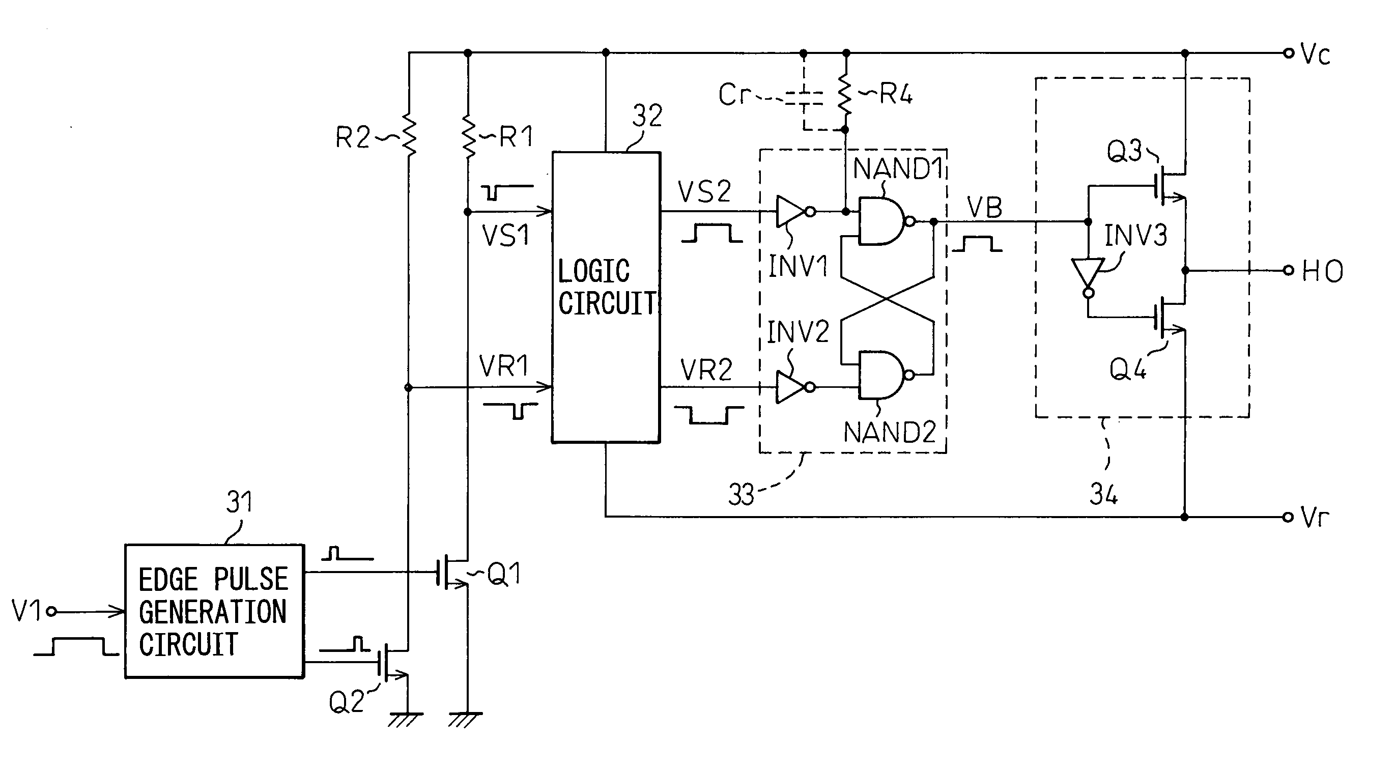
[0048] In the circuit in the first embodiment, when the output signal of INV1 is at the H level, an output voltage HO turns to the L level. In the circuit shown in FIG. 6, a parasitic capacitor Cr, when a diffused resistor is used for the setup resistor R4, is connected in parallel with the setup resistor R4. Because of this, a rush of current that flows through the parasitic capacitor Cr when the power is turned on bypasses the setup resistor R4. As a result, it is possible not only to suppress the voltage that develops across both ends of the setup resistor R4 due to the rush of current when the power is turned on but also to more surely return the output voltage of INV1 to the H level because of the rush of current that flows through the parasitic capacitor Cr, therefore, it is possible to surely return the output voltage HO to the L level.

[0049] As a result, when the circuit shown in FIG. 6 is applied to the drive circuit shown in FIG. 2 to drive the output device of the sustain...

third embodiment

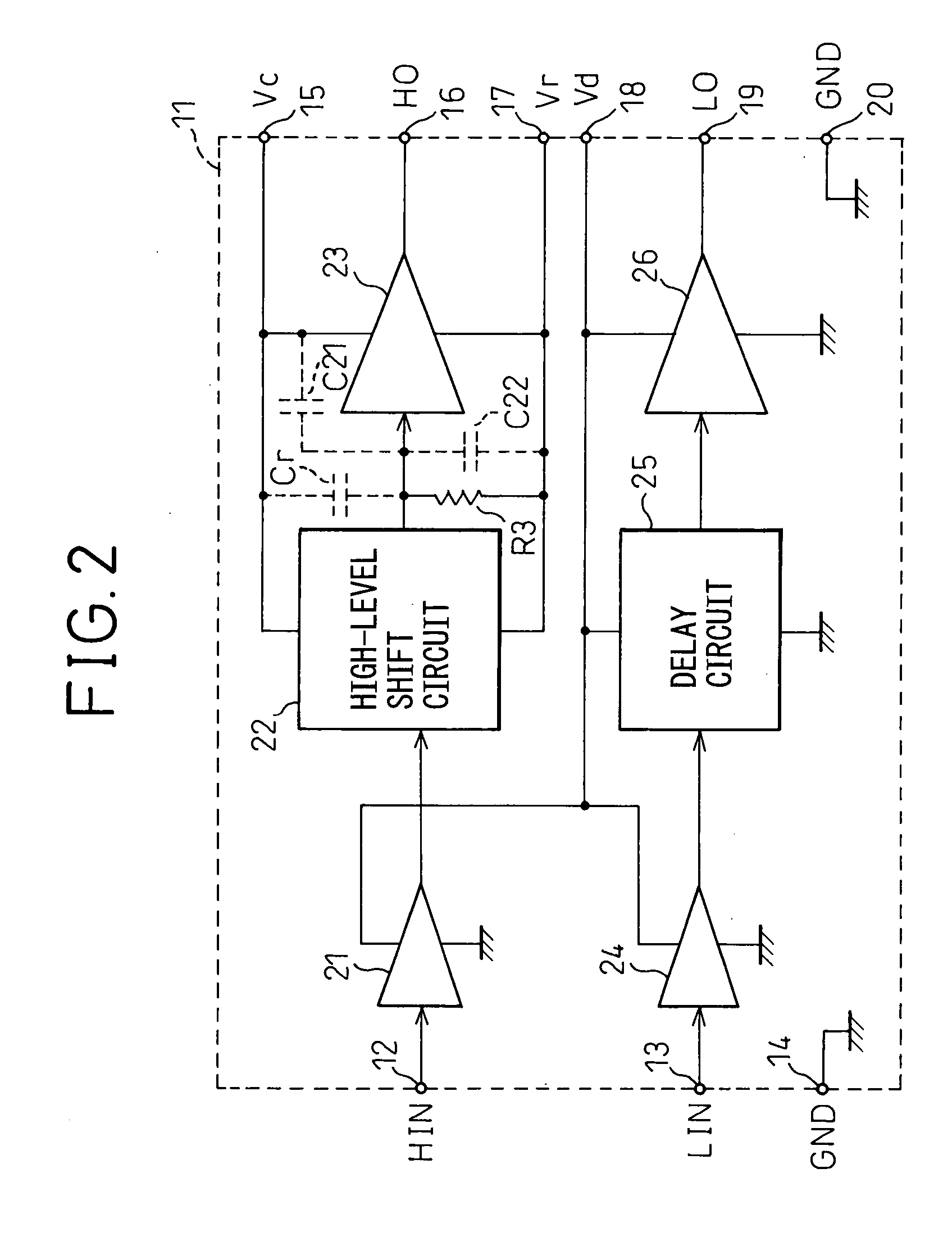
[0052]FIG. 8 is a diagram showing the configuration of a level shift circuit and an output amplifier circuit in a drive circuit for a display apparatus in the present invention, corresponding to FIG. 4. As is obvious from comparison with FIG. 4, the configuration is similar to that of the circuit shown in FIG. 4 but the difference lies in that a polysilicon resistor is used for the setup resistor R3.

[0053]FIG. 9A is a sectional view of a polysilicon resistor formed on an IC substrate and FIG. 9AB is a top view of a resistor pattern. As shown in FIG. 9A, a P-type diffusion layer 52 is provided on a P-type substrate 51 and a polysilicon layer 53 is provided thereon. The polysilicon layer 53 has a pattern 54 as shown in FIG. 9B and terminals T1 and T2 are provided on both ends of the pattern 54 as the terminals of the resistor. The resistance is determined based on the length of the pattern 54. Here, the P-type diffusion layer 52 is connected to the reference voltage line Vr but not to...

fourth embodiment

[0059] In the circuit in the fourth embodiment, a signal VR3 is generated by delaying a reset signal VR2 output from a logic circuit 32 and the signal VR3 is inputted to the flip-flop circuit 33. As a result, the output signal of a second NAND circuit NAND 2 (the input signal of the first NAND circuit NAND 1) is delayed compared to the signal inputted to the first NAND circuit NAND 1 from the set signal VS2 output from the logic circuit 32 via INV1 by the amount according to the time to pass through the reset delay circuit 35. Therefore, the time at which an output signal VB of the flip-flop circuit 33 is set by the set signal VS2 is ahead of the time at which the output signal VB is reset by the reset signal VR2. Because of this, even if the set signal VS2 and the reset signal VR2 are output simultaneously such as when the power supply voltage Vc is turned on, the reset signal VR2 to be inputted later determines the voltage level of the output signal VB of the flip-flop circuit 33,...


PUM


Abstract

A drive circuit, for a display apparatus, capable of preventing the occurrence of malfunctions, when the power is turned on, and the destruction of an output device. The drive circuit comprises an edge pulse generation circuit for generating a front edge pulse and a back edge pulse of an input signal, a first level shift circuit for converting the front edge pulse, a second level shift circuit for converting the back edge pulse, a logic circuit, a flip-flop circuit, a setup resistor connected to a signal line in the flip-flop circuit or in the post stage of the flip-flop circuit, an output amplifier circuit connected to the post stage of the setup resistor, and an output device connected to the output amplifier circuit, wherein a capacitive load of the display apparatus is driven by the output device and the setup resistor is connected between the power supply signal line of the output amplifier circuit and the signal line.

Description

BACKGROUND OF THE INVENTION [0001] The present invention relates to a drive circuit for a display apparatus and to a plasma display apparatus and, more particularly, to an improvement in the timing of a drive signal for causing a sustain discharge to occur. [0002] The plasma display apparatus has been put into practical use as a flat display and is expected to act as a thin display with high luminance. FIG. 1 is a diagram showing the general configuration of a conventional three-electrode AC-driven type plasma display apparatus. As shown schematically, the plasma display apparatus comprises a plasma display panel (PDP) 1 constituted of two substrates having a plurality of X electrodes (X1, X2, X3, . . . , Xn) and a plurality of Y electrodes (Y1, Y2, Y3, . . . , Yn) arranged adjacently, a plurality of address electrodes (A1, A2, A3, . . . , Am) arranged in the direction perpendicular to that of the X and Y electrodes, and phosphors arranged at the crossings of the electrodes, wherein...

Claims


Application Information

Patent Timeline
IPC IPC(8): G09G3/28G09G3/288G09G3/20G09G3/291G09G3/294G09G3/296G09G3/298H03K17/00H03K17/08H03K17/687
CPCG09G3/296G09G2330/04G09G2330/028G09G2330/025B42F1/02B42F15/066B42P2201/10B42P2241/10F16B2/16
Inventor ONOZAWA, MAKOTOOHKI, HIDEAKIOKADA, YOSHINORI
Owner FUJITSU HITACHI PLASMA DISPLAY LTD
Why Eureka
Try Eureka