CMOS image sensor which reduced noise caused by charge pump operation

a technology of image sensor and charge pump operation, which is applied in the field of complementary metal oxide semiconductor (cmos) image sensor, can solve the problems of inconvenient technology and problem of noise caused by pump operation, and achieve the effect of reducing nois

Inactive Publication Date: 2006-01-05
FUJITSU LTD
View PDF13 Cites 11 Cited by
  • Summary
  • Abstract
  • Description
  • Claims
  • Application Information

AI Technical Summary

Benefits of technology

[0018] At another aspect, the present invention offers a method of reducing a noise caused by a pumping operation including a step of preventing affects of a noise caused by a pumping operation of a charge pump type voltage up circuit to a correlated double sampling, in a CMOS image sensor comprising arrays of picture element circuits, a correlated double sampling unit of correlated double sampling one array of picture elements line and a charge pump type voltage up unit supplying a predetermined upped voltage up picture element circuits for forming an array.

Problems solved by technology

In this case, however, a noise caused by a pumping operation becomes a problem.
Therefore, this technology is inconvenient.
However, it is assumed that a technology of reducing the noise cased by a pumping operation in a CMOS image sensor using a circuit in which a voltage up is caused by a charge pump has not been disclosed.

Method used


Image

  • CMOS image sensor which reduced noise caused by charge pump operation
  • CMOS image sensor which reduced noise caused by charge pump operation
  • CMOS image sensor which reduced noise caused by charge pump operation

Examples


Embodiment Construction

[0027] The following is the detailed explanation of the present invention in reference to preferred embodiments of the present invention and attached drawings. Meanwhile, in a plurality of drawings, like reference numerals denote like elements.

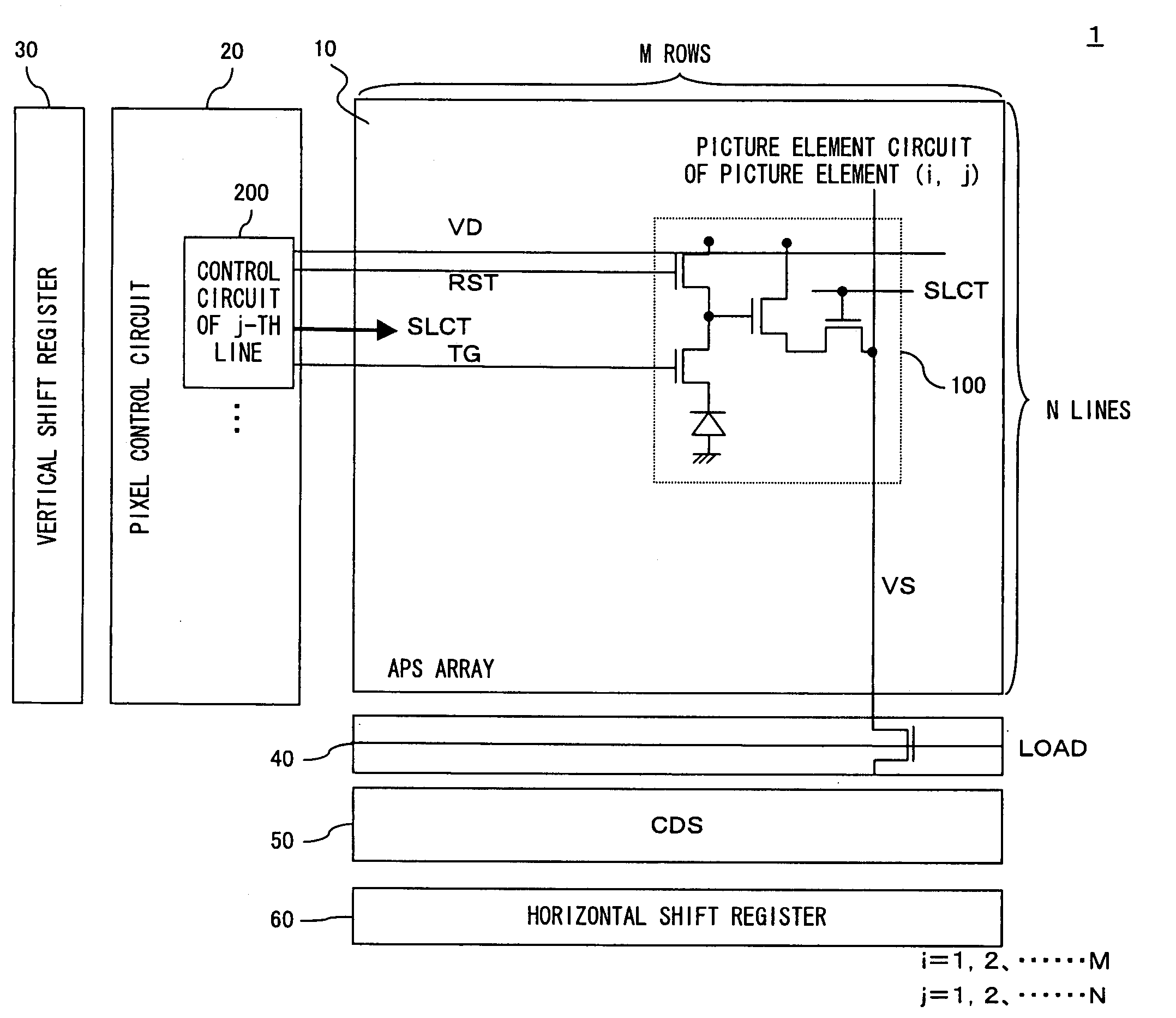
[0028]FIG. 1 is a block diagram conceptually showing the configuration of a CMOS image sensor that reduces the noise generated by a pumping operation and uses a charge pump type voltage up circuit according to one preferred embodiment of the present invention. In FIG. 1, a CMOS image sensor 1 generally comprises a pixel control circuit 20 for controlling and driving an active pixel sensor (APS) forming an APS array 1 and an APS array 10, a vertical shift register 30 for storing a row address, a line loading circuit 40 for loading for each line the respective lines of the APS array 10 into a correlated double sampling (CDS) circuit 50 and a horizontal shift register 60 for storing a line address. The APS array 10 includes an array of the APS 1...


PUM


Abstract

A CMOS image sensor of the present invention comprises an array of a picture element circuit, a unit of correlated double sampling one picture element line of the array, a charge pump type voltage up unit of supplying a predetermined step-up voltage to the picture element circuit that forms an array and a prevention unit of preventing the noise caused by a pumping operation of the charge pump type voltage up unit. The prevention unit may be a prohibition unit of prohibiting a pumping operation of the charge pump type voltage up unit. In the case where the charge pump type voltage up unit comprises a voltage up circuit for assigning a voltage up output in accordance with an assigned clock and a clock generation circuit for generating a clock in such a way that the voltage up output matches with the predetermined upped voltage, the prohibition unit of prohibiting a pumping operation may comprise a not-assignment unit of not assigning an output of the clock generation unit to the voltage up circuit.

Description

CROSS-REFERENCE TO RELATED APPLICATIONS [0001] This application is based upon and claiming the benefit of priority from the prior Japanese Patent Application No. 2004-194753, filed in Jun. 30, 2004, the entire contents of which are incorporated herein by reference. BACKGROUND OF THE INVENTION [0002] 1. Field of the Invention [0003] The present invention relates to a complementary metal oxide semiconductor (CMOS) image sensor using a circuit in which a voltage up is caused by a charge pump. Specifically, it relates to a technology of reducing a noise caused by a charge pump operation in such a CMOS image sensor. [0004] 2. Description of the Related Art [0005] In order to secure a certain degree of image quality in a CMOS sensor, a high voltage greater than a power source voltage of the sensor is generally required. Therefore, a charge pump which is easily miniaturized and is easily implemented using an integrated circuit (IC), is often used to obtain the required high voltage. In thi...

Claims


Application Information

Patent Timeline
Patent Type & Authority Applications(United States)
IPC IPC(8): H04N5/335H01L27/146H04N5/357H04N5/374H04N5/376
CPCH04N5/355H04N5/378H04N5/3745H04N5/3575H04N25/57H04N25/616H04N25/77H04N25/75H04N25/60
Inventor YANAGISAWA, MAKOTOINOUE, TADAOFUNAKOSHI, JUN
Owner FUJITSU LTD
Why Eureka
Try Eureka