Multilayer ceramic device, method for manufacturing the same, and ceramic device

a ceramic device and multi-layer technology, applied in the field of multi-layer ceramic devices, can solve problems such as breaking the electric connection through, and achieve the effects of suppressing the disconnection trouble or breakage of the electric connection, reducing the thickness of the internal electrode, and suppressing the disconnection troubl

Inactive Publication Date: 2006-01-05
TDK CORPARATION
View PDF15 Cites 8 Cited by
  • Summary
  • Abstract
  • Description
  • Claims
  • Application Information

AI Technical Summary

Benefits of technology

[0010] In this multilayer ceramic device, the melting point of the material forming the electroconductive member is higher than that of the material forming the internal electrode, whereby the electroconductive member has the contraction percentage in baking smaller than that of the internal electrode. This results in relatively constricting the contraction of the electroconductive member in baking, so as to decrease the difference of contraction percentages in baking between the ceramic source bodies intended for the ceramic layers, and the electroconductive member in the through hole. As a result, the electroconductive member is prevented from deviating to one side in the through hole or from breaking apart on the way during the baking, and it then prevents the breakage of electric connection through the electroconductive member in the through hole. On the other hand, contraction of the internal electrode is relatively promoted in baking, so as to make the internal electrode thinner by baking. Therefore, this multilayer ceramic device successfully achieves secure electric connection through the electroconductive member in the through hole and reduction in the thickness of the internal electrode during manufacturing.
[0011] In the multilayer ceramic device according to the present invention, preferably, each of the electroconductive member and the internal electrode is made of a material containing at least one of silver and gold, and palladium, and a proportion of palladium in the material forming the electroconductive member is higher than a proportion of palladium in the material forming the internal electrode. Since the melting point of palladium (Pd) is higher than those of silver (Ag) and gold (Au), the melting point of the material forming the electroconductive member can be made higher than that of the material forming the internal electrode, by setting the proportion of Pd in the material forming the electroconductive member higher than the proportion of Pd in the material forming the internal electrode.
[0014] In this method for manufacturing the multilayer ceramic device, the melting point of the material forming the electroconductive member is higher than the melting point of the material forming the internal electrode, and the melting point of the material forming the internal electrode is higher than the temperature at which the ceramic laminate is baked; therefore, the electroconductive member has the contraction percentage in baking smaller than that of the internal electrode. Therefore, for the same reason as in the case of the aforementioned multilayer ceramic device, this method for manufacturing the multilayer ceramic device enables achievement of secure electric connection through the electroconductive member in the through hole and reduction in the thickness of the internal electrode during manufacturing.
[0017] In this multilayer ceramic device, the contraction percentage in baking of the electroconductive member is smaller than that of the internal electrode. This suppresses contraction of the electroconductive member in baking, so as to decrease the difference of contraction percentages in baking between the ceramic source body intended for the ceramic layer, and the electroconductive member in the through hole. As a result, it prevents the electroconductive member from deviating to one side in the through hole or from breaking apart on the way during baking, and thus suppresses the disconnection trouble or breakage of the electric connection through the electroconductive member in the through hole. Since this multilayer ceramic device eliminates the need for provision of the thick internal electrode in order to suppress the disconnection trouble in the through hole during the baking, it becomes feasible to achieve reduction in the thickness of the internal electrode. Since the internal electrode has the contraction percentage in baking larger than that of the electroconductive member, the contraction of the internal electrode is not significantly impeded, whereby the internal electrode can be made thinner by baking. Therefore, this multilayer ceramic device enables achievement of secure electric connection through the electroconductive member in the through hole and reduction in the thickness of the internal electrode during manufacturing.
[0020] The ceramic device according to the present invention may be characterized in that the ceramic material is the same as a ceramic material forming the ceramic layer. This configuration decreases the difference of contraction percentages in baking between the ceramic layer and the electroconductive member in the through hole.
[0023] In this ceramic device, the electroconductive member contains the electroconductive material and the ceramic material, whereby the electroconductive member has the contraction percentage in baking smaller than in the case without the ceramic material. Therefore, it results in making small the difference of contraction percentages in baking between the ceramic source body intended for the ceramic layer, and the electroconductive member in the through hole. In consequence, it prevents the electroconductive member from deviating to one side in the through hole or from breaking apart on the way during baking, and it thus suppresses the disconnection trouble or breakage of the electric connection through the electroconductive member in the through hole. Since this multilayer ceramic device eliminates the need for provision of the thick internal electrode in order to suppress the disconnection trouble in the through hole in baking, it becomes feasible to achieve the reduction in the thickness of the internal electrode. Since the content of the ceramic material in the internal electrode is smaller than that in the electroconductive member, the contraction percentage of the internal electrode in baking is larger than that of the electroconductive member, whereby the contraction of the internal electrode is not significantly impeded, so as to make the internal electrode thinner by baking. Therefore, the multilayer ceramic device enables achievement of secure electric connection through the electroconductive member in the through hole and reduction in the thickness of the internal electrode during manufacturing.

Problems solved by technology

Namely, since the electroconductive members in the through holes have the contraction percentage in baking greater than that of the ceramic source bodies intended for the ceramic layers, the electroconductive members tend to deviate to one side or break apart on the way in the through holes, so as to result in breaking the electric connection through the electroconductive members in the through holes.

Method used


Image

  • Multilayer ceramic device, method for manufacturing the same, and ceramic device
  • Multilayer ceramic device, method for manufacturing the same, and ceramic device
  • Multilayer ceramic device, method for manufacturing the same, and ceramic device

Examples


first embodiment

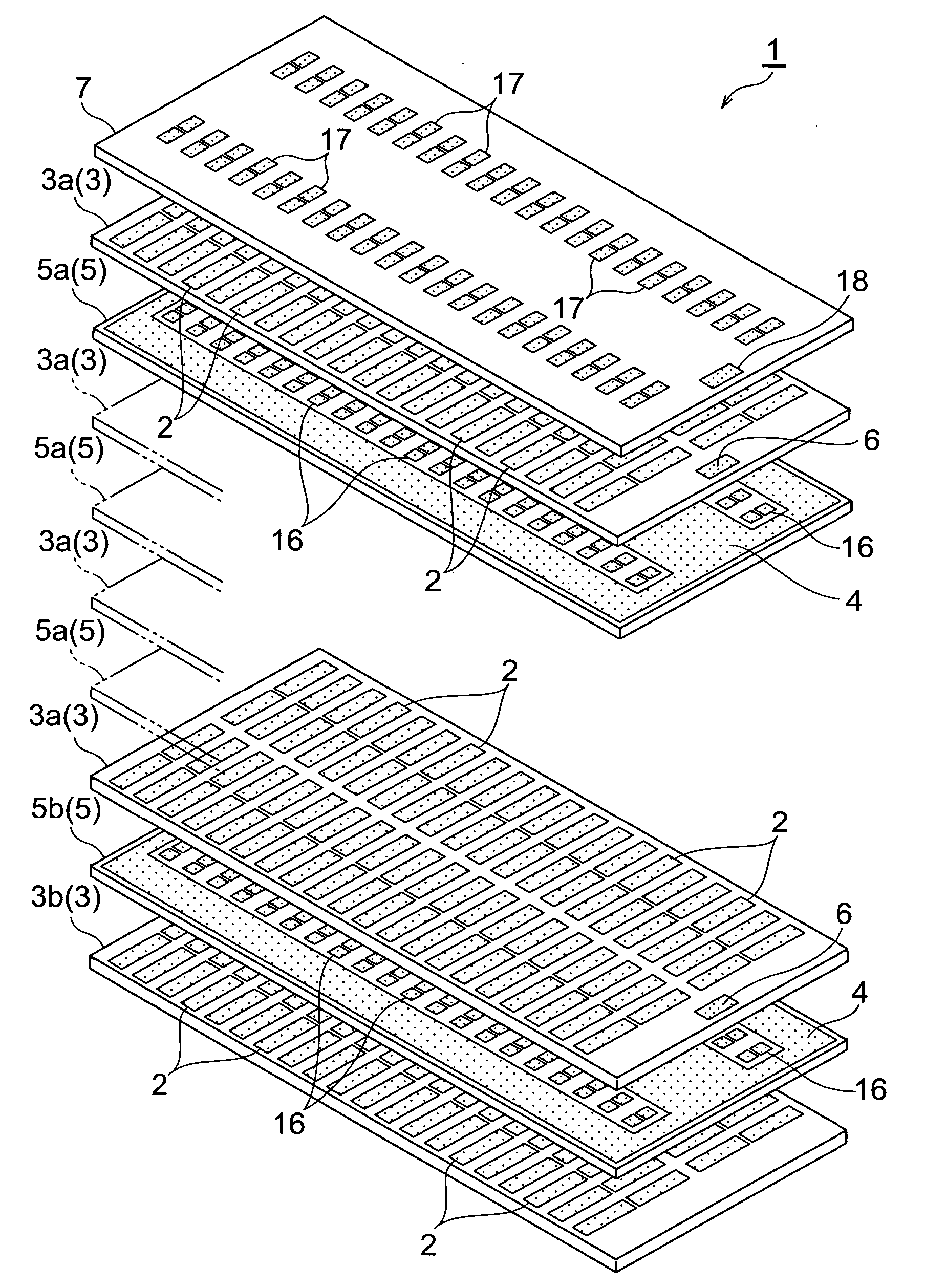
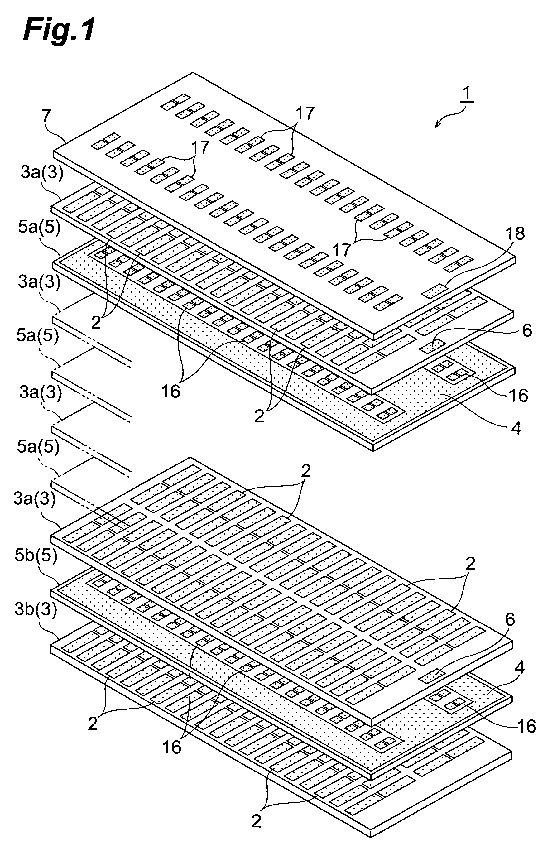
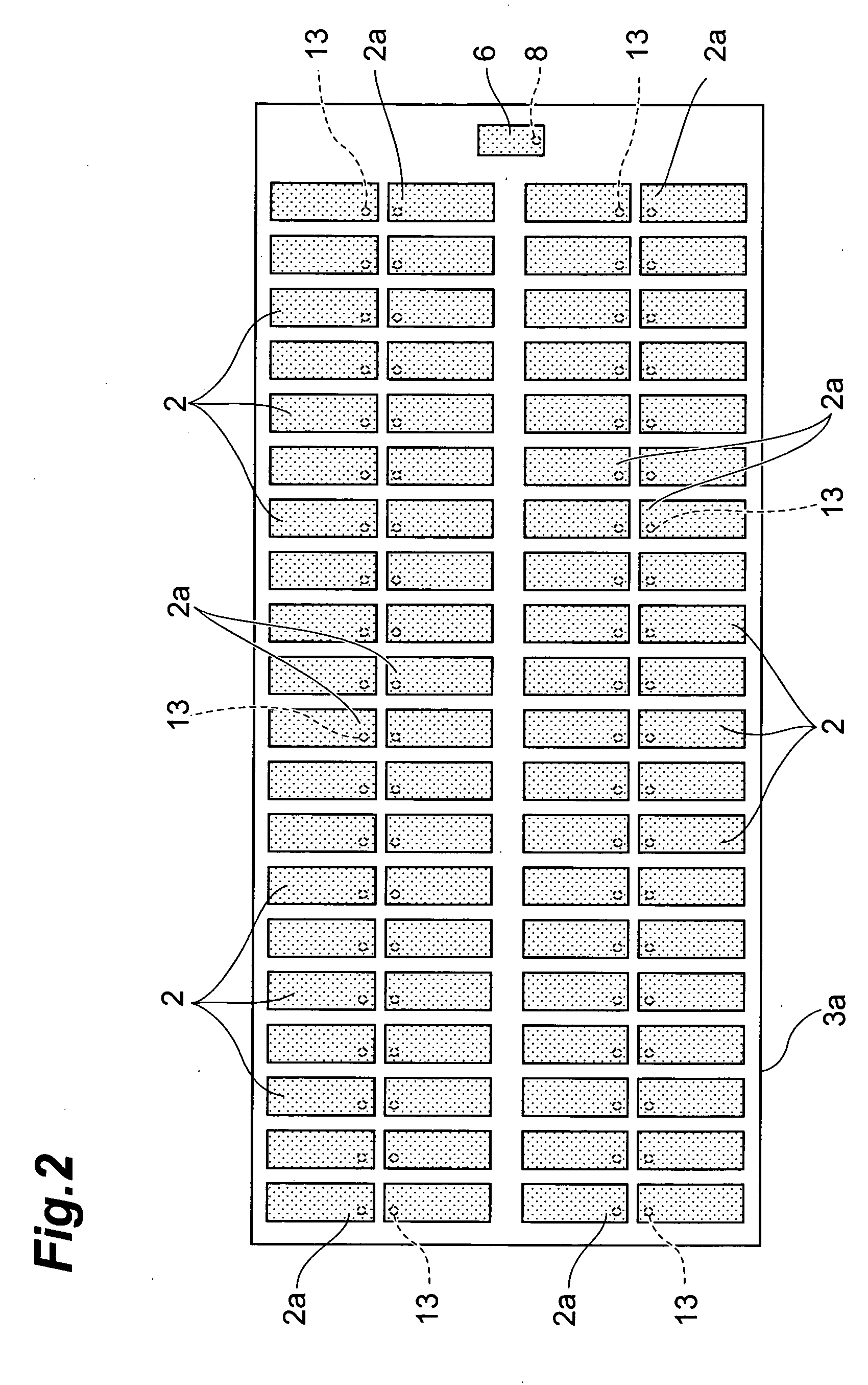
[0032] As shown in FIG. 1, the multilayer piezoelectric device (multilayer ceramic device) 1 of the first embodiment is constructed in a configuration wherein piezoelectric layers (ceramic layers) 3 with individual electrodes (internal electrodes) 2, and piezoelectric layers (ceramic layers) 5 with a common electrode (internal electrode) 4 are alternately stacked and wherein a piezoelectric layer (ceramic layer) 7 with terminal electrodes17, 18 is further stacked as the uppermost layer.

[0033] Each of the piezoelectric layers 3, 5, and 7 is made of a material consisting primarily of a ceramic such as lead zirconate titanate and is formed, for example, in a rectangular thin plate shape of “10 mm×30 mm, and 30 μm thick.” The individual electrodes 2 and common electrodes 4 are made of an electroconductive material consisting primarily of Ag and Pd, and are formed in a pattern by screen printing. This also applies to each of electrodes described below, except for terminal electrodes 17,...

second embodiment

[0061] The multilayer piezoelectric device (ceramic device) 1 according to the second embodiment is different in the material of the internal electrodes 2 and others and the material of the electroconductive members 14 from the multilayer piezoelectric device 1 of the first embodiment.

[0062] Namely, in the multilayer piezoelectric device 1 of the second embodiment, the individual electrodes 2 and common electrodes 4 are made of a material in which a common material is mixed in a metal material (electroconductive material), and thus have electric conductivity. This metal material consists primarily of Ag and Pd, and the common material is the same ceramic material as the material forming the piezoelectric layers 3, 5, 7. The content of the common material in the individual electrodes 2 and the common electrodes 4, as a mass percentage relative to the metal material, is, for example, 20% by mass relative to the metal material.

[0063] The electroconductive members 14 in the through ho...


PUM

PropertyMeasurementUnit
thickaaaaaaaaaa
temperatureaaaaaaaaaa
electroconductiveaaaaaaaaaa

Abstract

There is provided a multilayer ceramic device enabling achievement of secure electric connection via electroconductive members in through holes and reduction in the thickness of internal electrodes during manufacturing. In multilayer piezoelectric device 1, a melting point of a material of the electroconductive members in the through holes is higher than a melting point of a material of the internal electrodes 2 and others. For this reason, the electroconductive members in the through holes have a contraction percentage in baking smaller than that of the internal electrodes 2 and others. Therefore, contraction of the electroconductive members is relatively constricted in baking, so as to decrease the difference of contraction percentages in baking between green sheets intended for piezoelectric layers 3 and others, and the electroconductive members in the through holes. This results in preventing breakage of the electrical connection via the electroconductive members in the through holes. On the other hand, contraction of the internal electrodes 2 and others is relatively promoted in baking, so as to make the internal electrodes 2 and others thinner by baking.

Description

BACKGROUND OF THE INVENTION [0001] 1. Field of the Invention [0002] The present invention relates to a multilayer ceramic device, such as a multilayer piezoelectric device or a multilayer capacitor, and a method for manufacturing the same, and to a ceramic device. [0003] 2. Related Background Art [0004] One of the conventional multilayer ceramic devices is, for example, a multilayer piezoelectric device described in Japanese Patent Application Laid-Open No. 2002-254634. In this multilayer piezoelectric device, piezoelectric layers with a plurality of individual electrodes formed in a pattern, and piezoelectric layers with a common electrode formed in a pattern are alternately stacked, and individual electrodes aligned in the stack direction are connected by electroconductive members via through holes formed in the piezoelectric layers. [0005] In this piezoelectric device, lead wires for connection to a drive power supply are soldered to respective terminal electrodes formed on the u...

Claims


Application Information

Patent Timeline
Patent Type & Authority Applications(United States)
IPC IPC(8): B32B3/00B32B15/04B32B9/00
CPCH01G4/2325H01G4/30H01L41/0477Y10T428/24917H01L41/293H01L41/0474Y10T428/24926H01L41/083H10N30/874H10N30/877H10N30/50H10N30/063
Inventor SASAKI, SATOSHI
Owner TDK CORPARATION
Why Eureka
Try Eureka