Method for ultra thinning bumped wafers for flip chip

a technology of bumped wafers and flip chips, which is applied in the direction of basic electric elements, electrical apparatus, semiconductor devices, etc., can solve the problems of difficult bg tape manufacturing, difficult thinning, and formation of dimples (surface irregularities) on the back side of the wafer

Inactive Publication Date: 2006-01-05
AGENCY FOR SCI TECH & RES
View PDF8 Cites 15 Cited by
  • Summary
  • Abstract
  • Description
  • Claims
  • Application Information

AI Technical Summary

Benefits of technology

[0011] A principal object of the present invention is to provide an effective and very manufacturable method for fabricating an ultra thin bumped wafer for flip chip application.

Problems solved by technology

For bump heights greater than 200 μm it is difficult to manufacture BG tapes with thicker cushioning layer thickness and hence thinning becomes very difficult.
The difference in the force exerted on the region with and without bumps leads to formation of dimples (surface irregularities) on the back side of the wafer.
With ultra thinning of bumped wafers the surface irregularities become the potential area of failures.
These tape contaminants adversely affect the Flip Chip interconnection process.
However, there are too many process steps, including ashing and resin curing, which require process optimization for different bump heights.
Since the wafer has dummy bumps, tape lamination cannot seal the edges resulting in grinded silicon particle and slurry contamination issues.
Disadvantages of this process include additional process steps and higher materials cost.
The process method for depositing the liquid material will have a lot of waste which will have impact on the cost.

Method used


Image

  • Method for ultra thinning bumped wafers for flip chip
  • Method for ultra thinning bumped wafers for flip chip
  • Method for ultra thinning bumped wafers for flip chip

Examples


Embodiment Construction

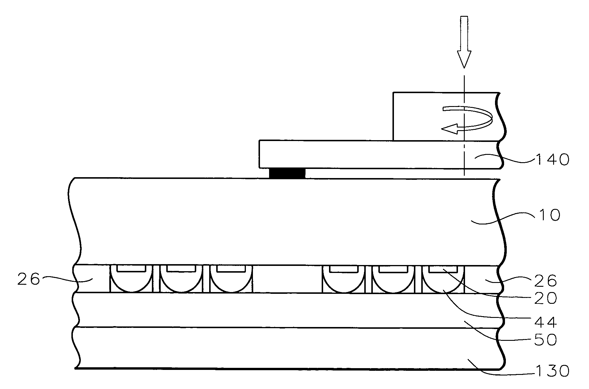
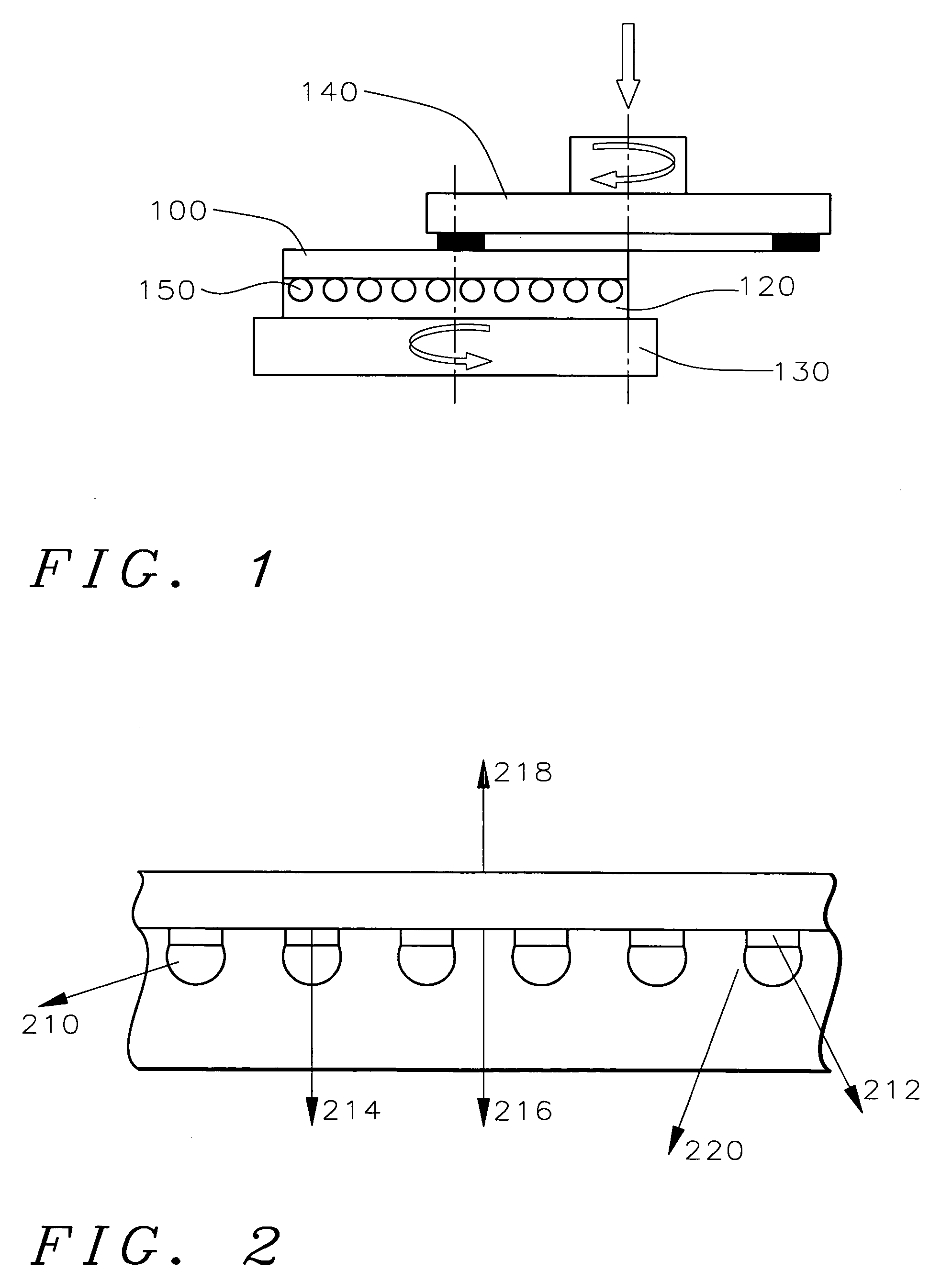
[0022] The present invention discloses a method for fabricating ultra thin bumped wafers for flip chip application. By this process, the number of steps for ultra thinning bumped wafers are reduced and ultra thinning is possible with high yield, excellent TTV control, and a wide range of bump heights The process does not require special BG tapes or special process parameter optimization and uses existing bumping and thinning equipment available in electronic packaging manufacturing facilities.

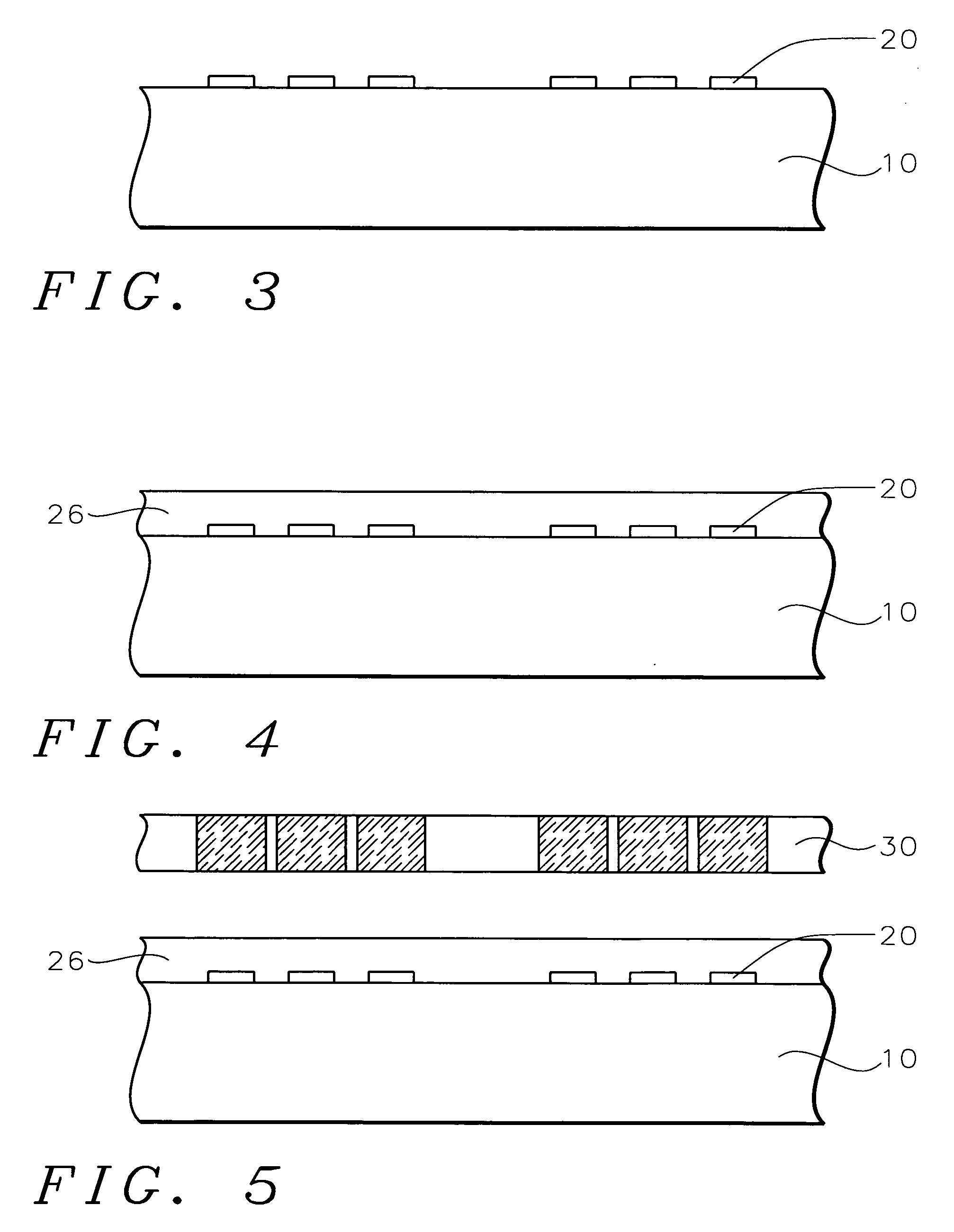
[0023] In the process of the present invention, a dry film laminated wafer is aligned to a bumping mask, exposed and developed. After developing, the solder paste is printed followed by reflow. BG tape is laminated on top of the dry film and the bumped wafer is thinned. After thinning, the wafer is attached to a carrier and then the BG tape is removed followed by dry film stripping. The thin bumped wafer is reflowed again for self-aligning of the solder balls to the UBM pads.

[0024] The proces...


PUM


Abstract

In an improved method for bumped wafer thinning, a wafer is provided having a front side and a back side wherein contact pads are formed on the top surface. A dry film is formed on the front side of the wafer and openings are provided in the dry film to the contact pads. Interconnections, such as solder bumps, are formed within the openings on the contact pads. A back grind tape or carrier is attached to the dry film and overlying the interconnections. Thereafter, the wafer is thinned from the back side of the wafer.

Description

BACKGROUND OF THE INVENTION [0001] 1) Field of the Invention [0002] The invention relates to a method of bumped wafer thinning, and more particularly, to a method of wafer thinning by a mechanical back grinding method. [0003] 2) Description of the Prior Art [0004] Conventional bumped wafer thinning starts with a bumped wafer that is laminated to a back grind (BG) tape to the front side of the wafer followed by backside wafer thinning. FIG. 1 illustrates the bumped wafer thinning process. The silicon wafer 100 has solder bumps 150 formed on a top side of the wafer and laminated to BG tape 120. The top of the wafer 100 is held to a vacuum chuck 130. Grinding wheel 140 is shown. The grinding wheel will thin the wafer from the backside. Challenges in conventional bumped wafer thinning include the following. 1.) Successful ultra thinning of a bumped wafer largely depends on the availability of back grind (BG) tape respective to the bump geometry. BG tapes are available in the market for ...

Claims


Application Information

Patent Timeline
Patent Type & Authority Applications(United States)
IPC IPC(8): H01L21/30H01L21/44
CPCH01L21/304H01L24/11H01L2924/0001H01L2224/13144H01L2224/131H01L2224/1131H01L2924/014H01L2224/13099H01L2924/01013H01L2924/01015H01L2924/01022H01L2924/01029H01L2924/01032H01L2924/01073H01L2924/01078H01L2924/01079H01L24/13H01L2924/01023H01L2924/00014H01L2224/05573H01L2224/05568H01L2224/05144H01L2224/05147H01L2224/05155H01L2224/05166H01L2224/05181H01L2224/05644H01L2224/05647H01L2224/05655H01L2224/05666H01L2224/05681H01L2224/1147H01L2224/11849H01L24/05H01L24/03H01L2224/0401
Inventor PERIASAMY, GANESH VETRIVELKRIPESH, VAIDYANATHAN
Owner AGENCY FOR SCI TECH & RES
Why Eureka
Try Eureka