Circuit board

a technology of circuit boards and components, applied in the direction of printed circuit aspects, electrical apparatus construction details, electric connection formation of printed elements, etc., can solve the problems of reduced cooling performance of circuit elements, poor heat dissipation, poor heat conductivity and heat dissipation of the connection portion between the cpu and the pins, etc., to achieve the effect of little improvemen

Inactive Publication Date: 2006-01-12
FUJITSU LTD
View PDF13 Cites 38 Cited by
  • Summary
  • Abstract
  • Description
  • Claims
  • Application Information

AI Technical Summary

Benefits of technology

[0011] The present invention has been made in view of the above circumstances, and provides a circuit board having a satisfactory characteristic of cooling a circuit element, without a constraint of mounting the circuit element on the rear surface of the substrate, without an interference with other parts, and without a trouble in the manufacturing process.

Problems solved by technology

When the solder 30 that flows and swells on the rear surface 20b is solidified, this constrains the mounting of elements onto the rear surface, causing problems.
When the circuit board 1 is disposed on a limited space, the solder reaching the rear surface 20b interferes with other parts, causing problems as well.
When a circuit board is mounted with a CPU (Central Processing Unit) having an extremely high heat dissipation value, or when a circuit board is mounted with many circuit elements requiring heat dissipation, the conventional technique shown in FIG. 1 cannot manage a rise (or a saturation) in a temperature of the substrate 20, which results in reduced performance of cooling the circuit elements.
Therefore, a connection portion between the CPU and the pins, that is, a portion of the adhesive, has poor heat conductivity and poor heat dissipation.
Consequently, despite the provision of the heat sink, the cooling effect is little improved.
The coating of an adhesive also becomes a trouble in the manufacturing process.

Method used


Image

  • Circuit board
  • Circuit board
  • Circuit board

Examples


first embodiment

[0037]FIG. 2 is a cross-sectional diagram of a circuit board according to the present invention.

[0038] In the following explanation, constituent elements having the same functions as those of the constituent elements shown in FIG. 1 are attached with like reference numerals. (the same applies hereinafter)

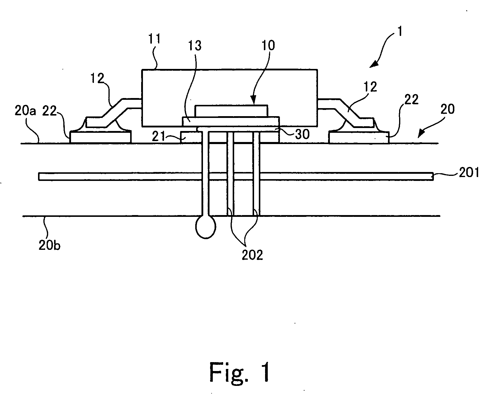
[0039] The circuit board 1 shown in FIG. 2 also has the semiconductor element 10 covered with the package 11, and the substrate, like the circuit board shown in FIG. 1. The semiconductor element 10 has plural leads 12, and the metal heat dissipation slug 13. The heat dissipation slug 13 shown in FIG. 2 is coated with a low melting-point material containing Bi (bismuth).

[0040] On the other hand, a pair of metal pads are provided at mutually opposite positions of a front surface and a rear surface of the substrate 20 shown in FIG. 2. These pads are also coated with a low melting-point material containing Bi of the front and rear surfaces, a surface on which the semiconductor element...

second embodiment

[0045]FIG. 3 is a cross-sectional diagram of a circuit board according to the present invention.

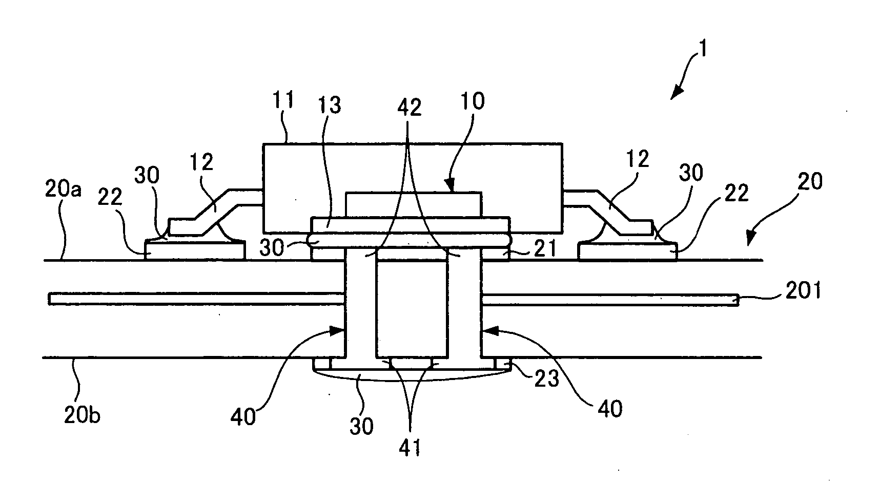
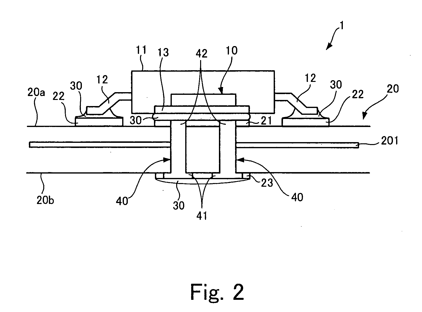
[0046] The circuit board 1 shown in FIG. 3 also has plural heat transfer sections 40. However, the head 41 of each heat transfer section 40 shown in FIG. 3 is soldered to the heat dissipation pad 21 in a state of being embedded in the heat dissipation pad 21, and the end part 42 is soldered to the heat dissipation rear-surface pad 23 in a state of being embedded in the heat dissipation rear-surface pad 23. Each heat transfer section 40 is accommodated in a through-hole that is mechanically formed on the substrate 20. A low melting-point material is not coated on any one of the heat dissipation slag 13, the heat dissipation pad 21, and the heat dissipation rear-surface pad 23 shown in FIG. 3. All the heads 41 and the ends 42 of the heat transfer sections 40 are coated with a low melting-point material containing Bi respectively. Therefore, the solder is melted at a temperature about the sa...

third embodiment

[0048]FIG. 4 is a cross-sectional diagram of a circuit board according to the present invention.

[0049] The semiconductor element 10 shown in FIG. 4 is a CPU having an extremely high heat dissipation value. According to the circuit board 1 shown in FIG. 4, the heat transfer sections 40 are also separated from the conductive layer 201 to avoid a rise in the temperature of the substrate, like the circuit board shown in FIG. 3. The circuit board 1 shown in FIG. 4 has a heat sink 50 disposed on the rear surface 20b. The heat sink 50 has plural fins 51 having a larger capacity than that of the heat dissipation rear-surface pad 23. Each heat transfer section 40 shown in FIG. 4 has a tube 430 that stretches from the heat dissipation rear-surface pad 23 in a thickness direction of the substrate 20. The peripheral surface of the tube 430 is soldered to the heat dissipation rear-surface pad 23.

[0050]FIG. 5 is a perspective diagram of a heat transfer section that is provided on the circuit boa...


PUM


Abstract

A circuit board includes a substrate having a pair of pads at mutually opposite positions of a front surface and a rear surface of the substrate; a circuit element having a heat dissipation part which is soldered to one of the pair of pads; and a heat transfer section which pierces through the substrate in a thickness direction, and both ends of which are soldered to the pair of pads respectively, wherein at least a part of the heat transfer section has a solid structure which prevents air from passing through between the front surface and the rear surface.

Description

BACKGROUND OF THE INVENTION [0001] 1. Field of the Invention [0002] The present invention relates to a circuit board having a substrate and a circuit element mounted on this substrate. [0003] 2. Description of the Related Art [0004] Along the increased sophistication of a circuit element, a heat dissipation value of the circuit element also increases. As a technique of cooling the circuit element, a metal heat dissipation pad (i.e., a slug) is provided on a portion (i.e., a rear surface) of the circuit element facing the substrate, and this heat dissipation slug is soldered to the metal pad disposed on the substrate, thereby releasing the heat from the circuit element. [0005]FIG. 1 is a cross-sectional diagram of a circuit board to which a heat dissipation slug of a semiconductor element and a pad of a substrate are soldered. [0006] A circuit board 1 shown in FIG. 1 has a semiconductor element 10 and a substrate 20. The semiconductor element 10 is covered with a package 11 which has...

Claims


Application Information

Patent Timeline
Patent Type & Authority Applications(United States)
IPC IPC(8): H05K7/20
CPCH05K1/0204H05K3/341H05K3/3447H05K2201/10689H05K2201/066H05K2201/10416H05K3/42
Inventor IKETAKI, KENJI
Owner FUJITSU LTD
Why Eureka
Try Eureka