
Transparent amorphous carbon structure in semiconductor devices

a technology of transparent amorphous carbon and semiconductor devices, applied in the field of semiconductor devices, can solve the problem that amorphous carbon masks are not applicable in some processes, and achieve the effect of low absorption property

Inactive Publication Date: 2006-01-12
MICRON TECH INC
View PDF24 Cites 14 Cited by
  • Summary
  • Abstract
  • Description
  • Claims
  • Application Information

AI Technical Summary

Benefits of technology

The transparent amorphous carbon layer enables accurate alignment mark reading and allows for specific thicknesses necessary in semiconductor manufacturing without the limitations of conventional masks, enhancing the precision and applicability of masking structures in semiconductor devices.

Problems solved by technology

However, an amorphous carbon mask at some thickness may have a high absorption of optical light, causing the amorphous carbon mask inapplicable for some processes.

Method used


Image

  • Transparent amorphous carbon structure in semiconductor devices
  • Transparent amorphous carbon structure in semiconductor devices
  • Transparent amorphous carbon structure in semiconductor devices

Examples


Embodiment Construction

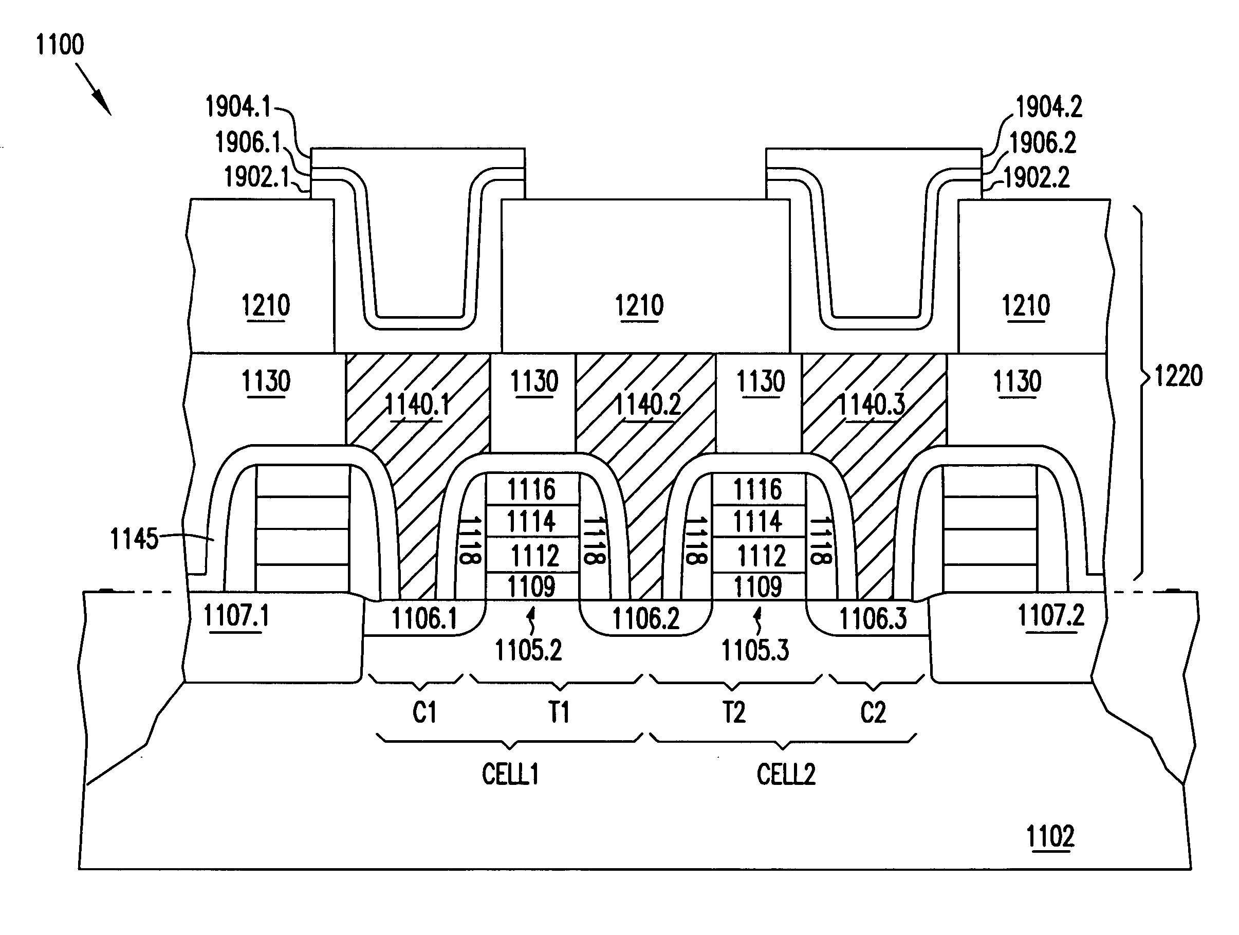
[0016] The following description and the drawings illustrate specific embodiments of the invention sufficiently to enable those skilled in the art to practice the invention. Other embodiments may incorporate structural, logical, electrical, process, and other changes. In the drawings, like numerals describe substantially similar components throughout the several views. Examples merely typify possible variations. Portions and features of some embodiments may be included in or substituted for those of others. The scope of the invention encompasses the full ambit of the claims and all available equivalents.

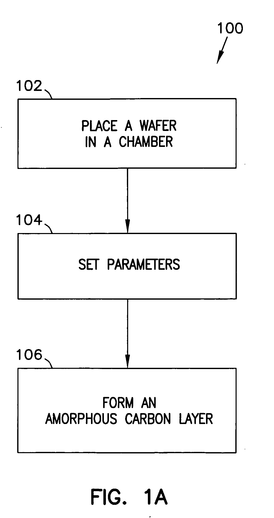
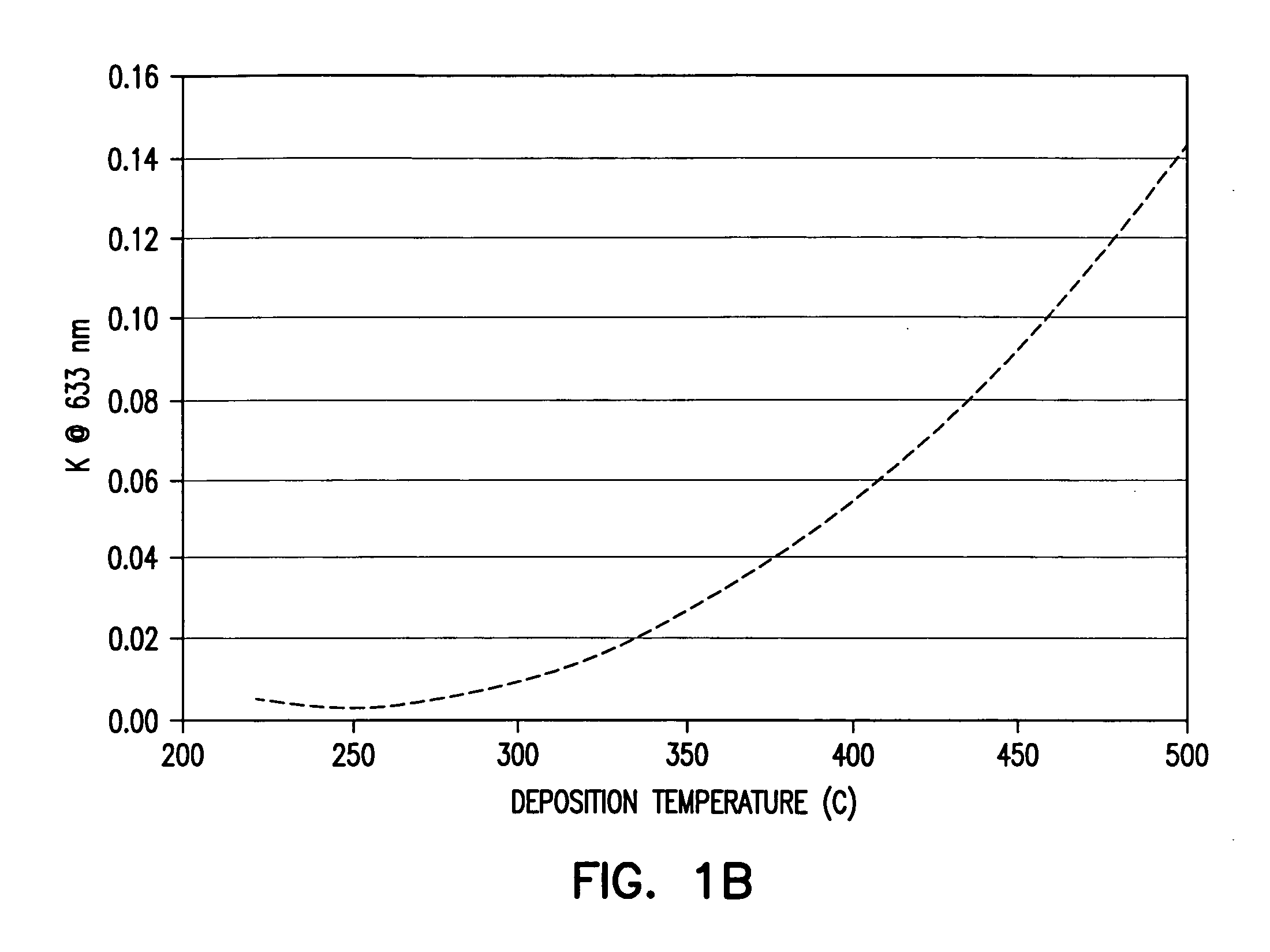
[0017]FIG. 1A is flowchart showing a method of forming an amorphous carbon layer according to an embodiment of the invention. Method 100 forms an amorphous carbon layer having a low absorption coefficient such that the amorphous carbon layer is transparent in visible light range.

[0018] The visible light range is the range (optical range) of the electromagnetic spectrum having light...


PUM

PropertyMeasurementUnit
wavelengthaaaaaaaaaa
wavelengthsaaaaaaaaaa

Abstract

A transparent amorphous carbon layer is formed. The transparent amorphous carbon layer has a low absorption coefficient such that the amorphous carbon is transparent in visible light. The transparent amorphous carbon layer may be used in semiconductor devices for different purposes. The transparent amorphous carbon layer may be included in a final structure in semiconductor devices. The transparent amorphous carbon layer may also be used as a mask in an etching process during fabrication of semiconductor devices.

Description

RELATED APPLICATIONS [0001] This application is a Divisional of U.S. application Ser. No. 10 / 661,379, filed Sep. 12, 2003. [0002] This application is related to the following co-pending and commonly assigned application; attorney docket number 303.869US1, application Ser. No. 10 / 661,100, filed Sep. 12, 2003, entitled “MASKING STRUCTURE HAVING MULTIPLE LAYERS INCLUDING AN AMORPHOUS CARBON LAYER” which is hereby incorporated by reference.FIELD OF INVENTION [0003] The present invention relates generally to semiconductor devices, more particularly to masking structures in the semiconductor devices. BACKGROUND [0004] Semiconductor devices such as memory devices reside in many computers and electronic products to store data. A typical semiconductor device has many layers of different materials formed on a semiconductor wafer. [0005] During manufacturing, the layers go through many processes. For example, a patterning process puts patterns on the layers. Some patterning processes use a mas...

Claims


Application Information

Patent Timeline
Patent Type & Authority Applications(United States)
IPC IPC(8): H01L21/469H01L21/4763H05H1/00G03C5/00H01L21/31H01L21/314H10B12/00
CPCH01L21/0237H01L21/02439H01L21/02505H01L21/02527H01L27/10852H01L21/0332H01L21/3081H01L21/3146H01L21/0262H01L21/02274H01L21/02115H01L21/0214H01L21/022H10B12/033H01L21/02126H01L21/02422
Inventor YIN, ZHIPINGLI, WEIMIN
Owner MICRON TECH INC
Features
  • Generate Ideas
  • Intellectual Property
  • Life Sciences
  • Materials
  • Tech Scout
  • Unparalleled Data Quality
  • Higher Quality Content
  • 60% Fewer Hallucinations
Learn More