Method for recycling/reclaiming a monitor wafer

Inactive Publication Date: 2006-01-12
TEXAS INSTR INC
View PDF16 Cites 26 Cited by
  • Summary
  • Abstract
  • Description
  • Claims
  • Application Information

AI Technical Summary

Benefits of technology

[0006] To address the above-discussed deficiencies of the prior art, the present invention provides a method for recycling/reclaiming a monitor wafer and a method for testing a manufacturing process. The method for recycling/reclaiming the monitor wafer, among other steps, includes providing a monitor wafer having a number of front surface defects thereon, and annealing the monitor wafer in a presence of an inert gas to correct one or more of the number of front surface defects.
[0007] The method for testing a manufacturing proces

Problems solved by technology

However, if the specific manufacturing step being tested does not achieve its intended purpose, the manufacturing step may be tweaked and tested again, without subjecting actual device wafers to the unsatisfactory manufacturing step.
The industry, as a result of the extreme number and cost of the monitor wafers being used, currently attempts to recycle or reclaim these used monitor wafers.
However, conventional technologies do not always tho

Method used


Image

  • Method for recycling/reclaiming a monitor wafer
  • Method for recycling/reclaiming a monitor wafer

Examples


Embodiment Construction

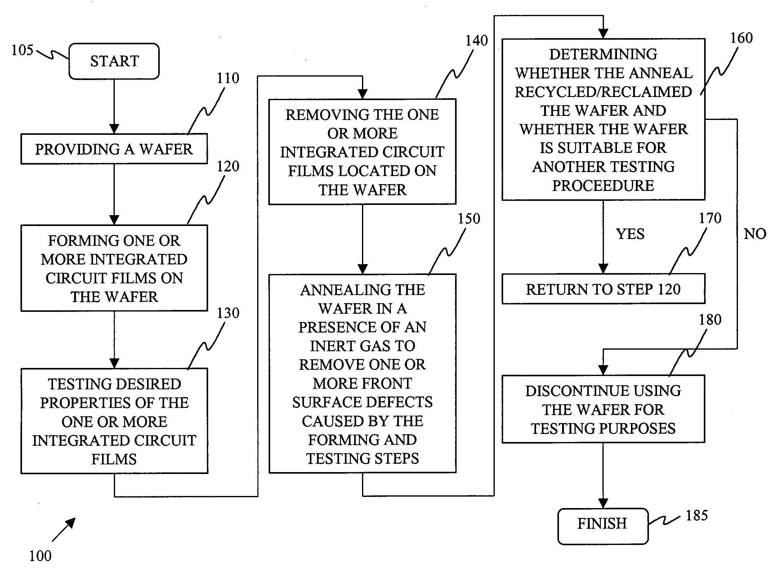
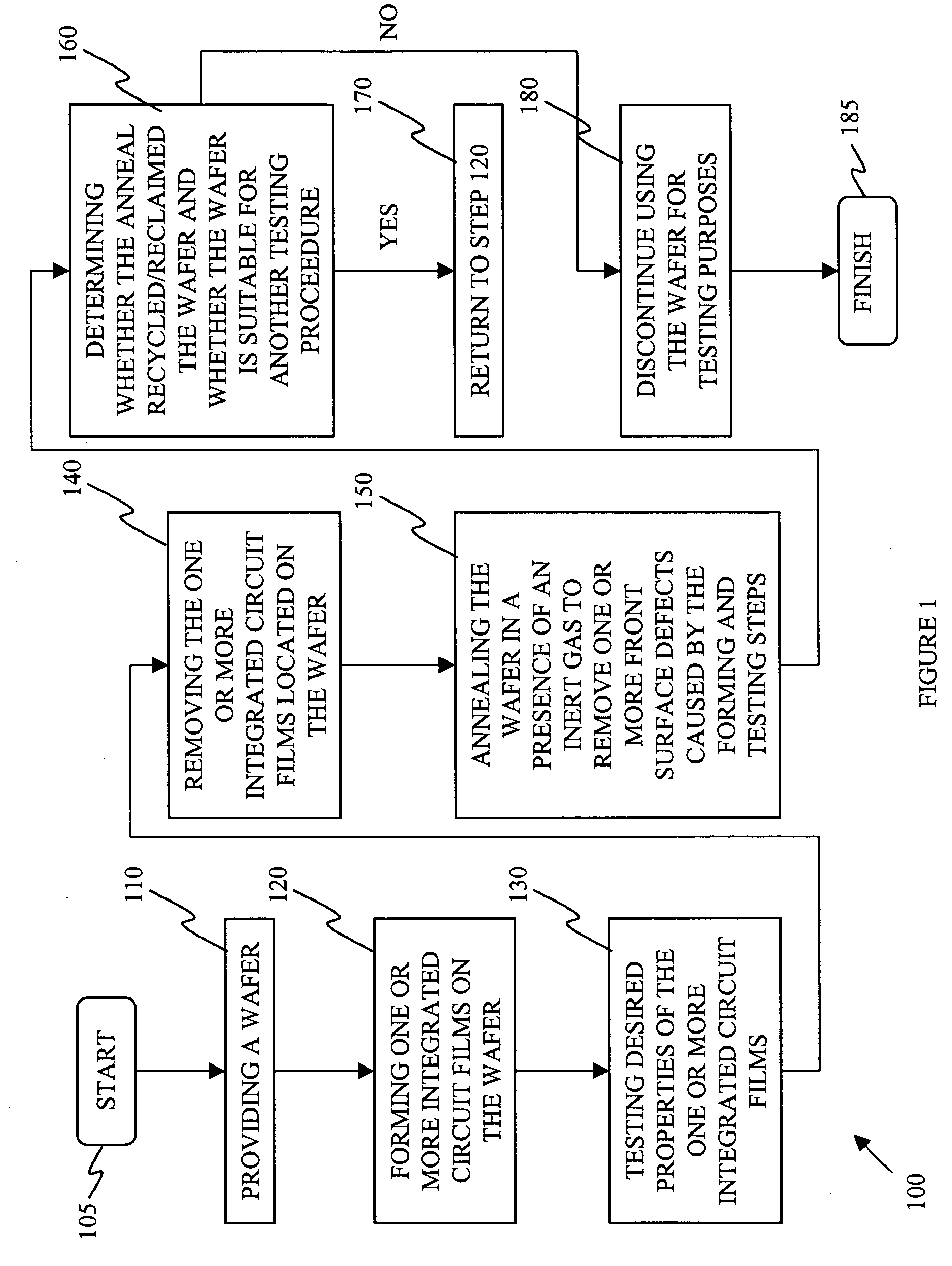
[0011] The present invention, in contrast to the prior art, begins with the unique recognition that if front surface defects on a monitor wafer caused during either the formation of the integrated circuit (IC) films on the monitor wafers or the testing of those films can be corrected, the effective useful life of the monitor wafer can be greatly increased. Namely, the present invention has recognized that if the front surface effects can be corrected, less lapping and polishing of the monitor wafer is required to sufficiently correct those front surface defects during the recycling / reclamation process. Therefore, the monitor wafer, and more specifically the thickness of the monitor wafer, withstands many more recycling / reclamation processes before being unsuitable for additional testing purposes.

[0012] Given the aforementioned recognition, the present invention observed that by annealing the monitor wafer in a presence of an inert gas, one or more of the front surface defects creat...


PUM


Abstract

The present invention provides a method for recycling/reclaiming a monitor wafer and a method for testing a manufacturing process. The method for recycling/reclaiming the monitor wafer, among other steps, includes providing a monitor wafer having a number of front surface defects thereon (110), and annealing the monitor wafer in a presence of an inert gas to correct one or more of the number of front surface defects (150).

Description

TECHNICAL FIELD OF THE INVENTION [0001] The present invention is directed, in general, to a method for manufacturing an integrated circuit and, more specifically, to a method for recycling / reclaiming a monitor wafer used in the manufacture of an integrated circuit. BACKGROUND OF THE INVENTION [0002] In practical semiconductor fabrication, hundreds and hundreds of individual manufacturing steps are required to convert a bare silicon wafer into one or more operational integrated circuits (ICs). In an effort to save time and money, after each individual manufacturing step is set up a monitor or test wafer is processed through the given manufacturing step to examine whether the manufacturing step achieves its intended purpose. If the specific manufacturing step being tested achieves its intended purpose, then the manufacturer is confident that actual device wafers may be subjected to the manufacturing step. However, if the specific manufacturing step being tested does not achieve its in...

Claims


Application Information

Patent Timeline
IPC IPC(8): H01L21/322
CPCH01L21/02032H01L22/34H01L21/3225H01L21/02079
Inventor BARRETT, GARY C.SUCHER, BRADLEY D.CARR, COLIN L.
Owner TEXAS INSTR INC
Why Eureka
Try Eureka