LED chip capping construction

a technology of led chip and capping, which is applied in the direction of discharge tube/lamp details, discharge tube luminescnet screens, electric discharge lamps, etc., can solve the problem of reducing the luminance of led, and achieve the effect of inhibiting the creation of diaphragms of strange colors

Inactive Publication Date: 2006-01-19
TAIWAN OASIS TECH CO LTD
View PDF7 Cites 43 Cited by
  • Summary
  • Abstract
  • Description
  • Claims
  • Application Information

AI Technical Summary

Benefits of technology

[0007] The primary purpose of the present invention is to provide a chip capping construction for a light emitting diode that effectively inhibit the creation of diaphragm of strange color. To achieve the purpose, additional to the basic construction of having fixed a chip and a fluorescent material to the carrier of the LED and a golden plated wire to connect the electrode layer of the chip and the conductors, a transparent transition layer is capped on the top of the chip, and a functional layer mixed with fluorescent material is further capped on the transition layer. The thickness of the functional layer at where in relation to the top layer of the chip is greater than that in relation to the peripheral of the chip so that the convex functional layer balances the incorporation of wavelength of the lights on the top layer of the chip and on the peripheral of the chip respectively with that of the fluorescent material. Of course, another convex light penetration layer may further cap on the functional layer to provide proper protection for the functional layer, the transitional layer and the chip.

Problems solved by technology

Furthermore, the capping on the chip with the white insulation glue also reduces the luminance of the LED.

Method used


Image

  • LED chip capping construction
  • LED chip capping construction
  • LED chip capping construction

Examples


Embodiment Construction

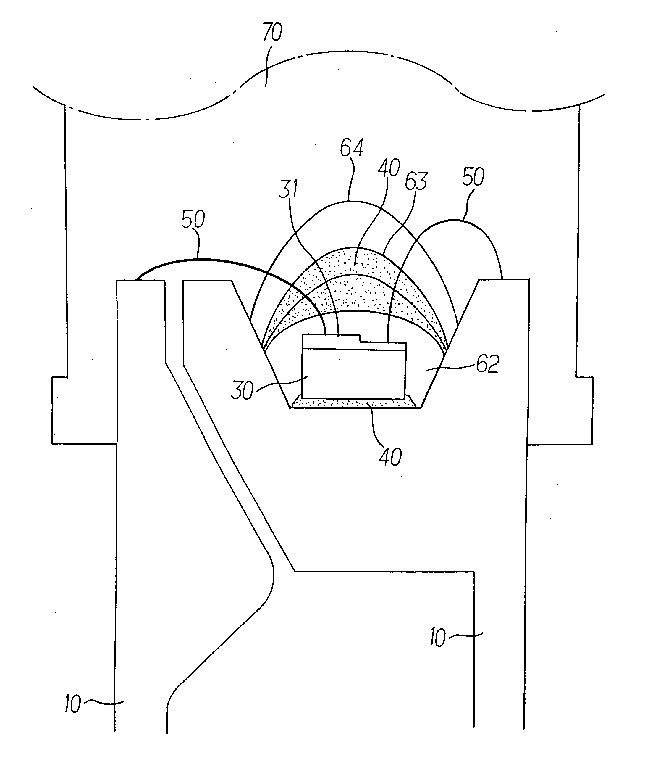
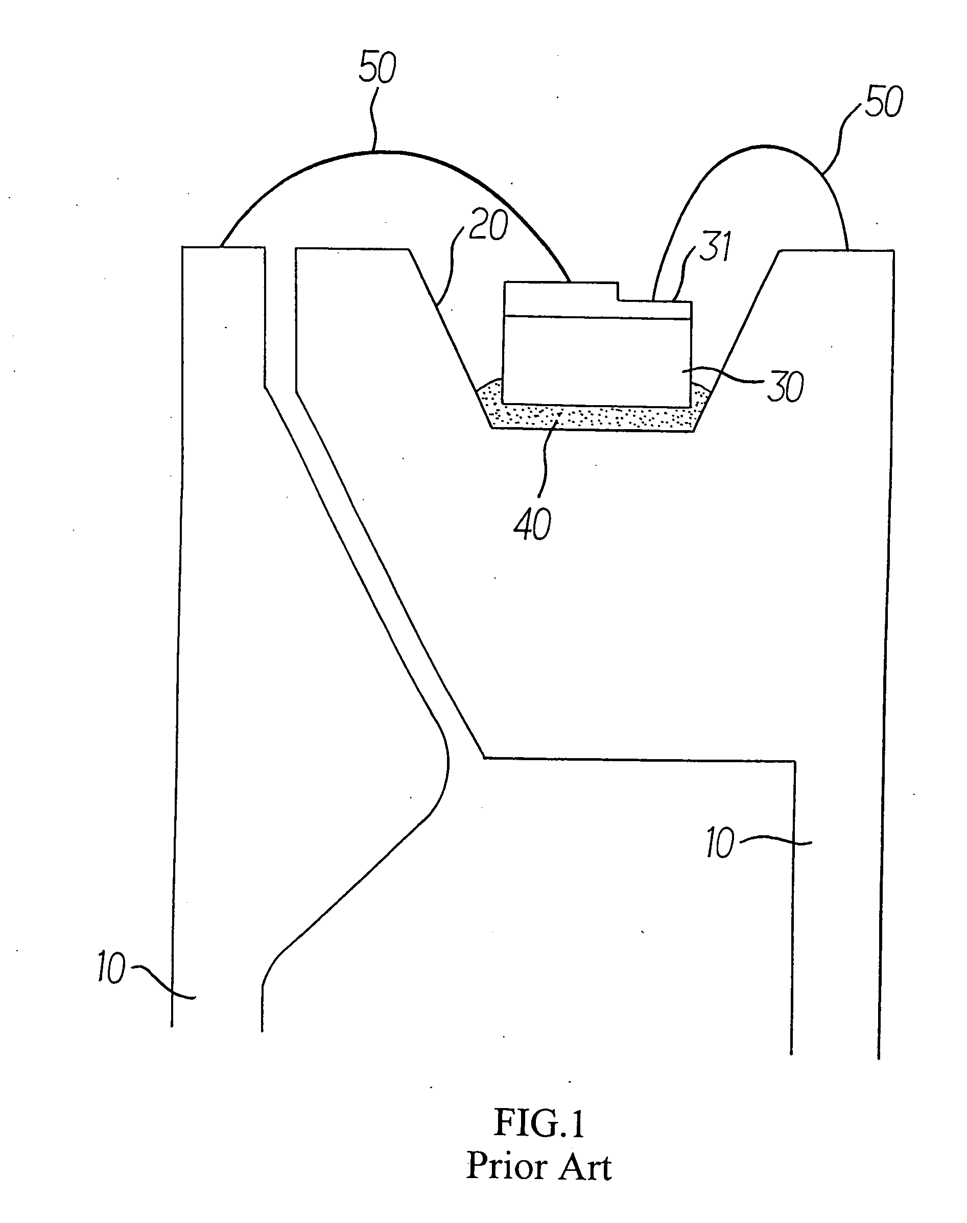
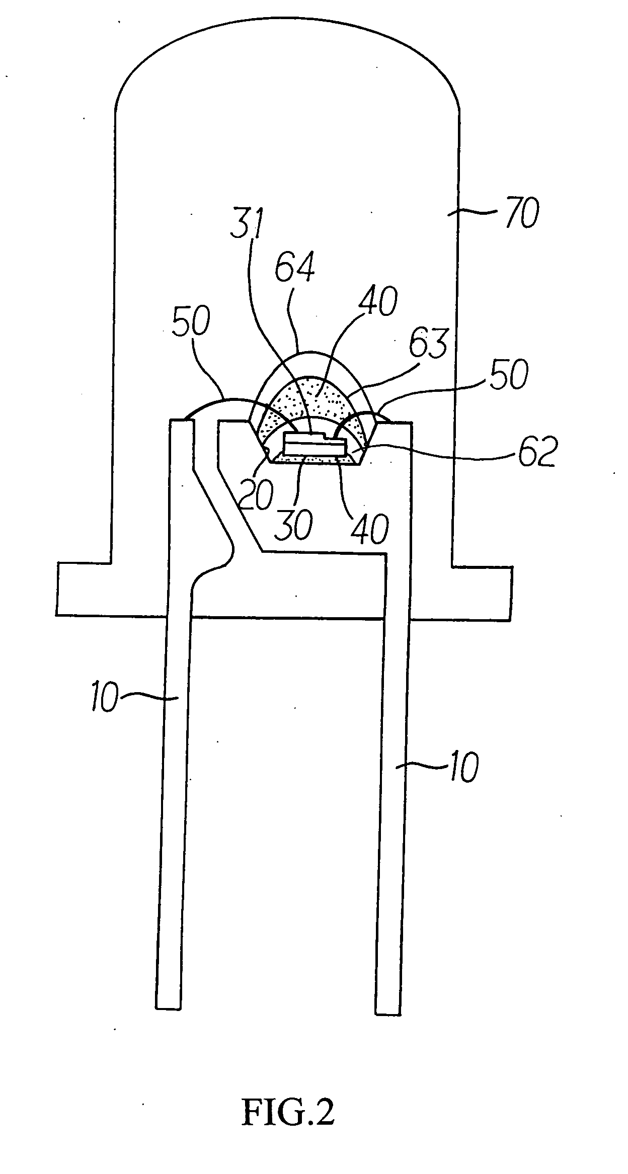
[0012] Referring to FIG. 2 for a basic construction of a light emitting diode of the present invention, a packaging 70 contains multiple conductors 10 of different polarities and a carrier 20. The packaging 70 is made of epoxy or a transparent material. A chip 30 and a fluorescent material 40 are placed in the carrier. A golden plated wire 50 connects an electrode layer 31 of the chip 30 and those conductors 10. Accordingly, once those conductors 10 are conducted, the light emitted form the chip 30 passing through the fluorescent material is incorporated with the wavelength of the fluorescent material 40 to form a specific light color. Also as illustrated in FIG. 3, the top of the chip 30 is capped with a transparent transitional layer 62. The top of the transparent transition layer 62 is capped with a functional layer 63 mixed with fluorescent material 40. In the preferred embodiment, the transparent transition layer 62 is related to a convex structure of hardened transparent insul...


PUM


Abstract

A chip capping construction for a light emitting diode having capped a transparent transitional layer on the top of the chip; a convex functional layer mixed with fluorescent material being capped on the top of the transparent transitional layer; the thickness at where the functional layer in relation to the top layer of the chip being greater than that of the functional layer in relation to the peripheral of the chip; and the greater thickness balancing the wavelength incorporation of the fluorescent material respectively with the top layer and the peripheral layer of the chip to effectively inhibit the creation of diaphragm of strange color.

Description

BACKGROUND OF THE INVENTION [0001] (a) Field of the Invention [0002] The present invention is related to an LED chip capping technology, and more particularly, to one that effectively eliminate diaphragm of strange color. [0003] (b) Description of the Prior Art [0004] As illustrated in FIG. 1 of the accompanying drawings for a schematic view of a construction of a light emitting diode (LED) providing specific light color effects by having the light emission from the chip incorporated with wave length of fluorescent material, the LED relates to a packaging containing conductors 10 of different polarities and a carrier 20. The carrier 20 is fixed with a chip 30 and a fluorescent material 40 while an electrode layer 31 of the chip 30 and the conductors 10 are connected by means of a golden plated wire 50. [0005] Once the conductors 10 are conducted, light emitted from the chip 30 passing through the fluorescent material 40 is incorporated with the wavelength of the fluorescent material...

Claims


Application Information

Patent Timeline
Patent Type & Authority Applications(United States)
IPC IPC(8): H01L33/00H01L33/50H01L33/54
CPCH01L33/505H01L33/54H01L33/507H01L2224/48091H01L2924/181H01L2224/48247H01L2224/48257H01L2224/49107H01L2224/8592H01L2924/00014H01L2924/00012
Inventor LEE, MING-SHUNSUNG, PING-RU
Owner TAIWAN OASIS TECH CO LTD
Why Eureka
Try Eureka