Voltage random access memory (VRAM)

Inactive Publication Date: 2006-01-26
KENET
View PDF4 Cites 1 Cited by
  • Summary
  • Abstract
  • Description
  • Claims
  • Application Information

AI Technical Summary

Benefits of technology

[0017]FIG. 7 illustrates another implementation of a VRAM cell providing a coarse

Problems solved by technology

However, certain types of circuits, such as charge to digital converters, may require generation of many such analog voltages.
Ev

Method used


Image

  • Voltage random access memory (VRAM)
  • Voltage random access memory (VRAM)
  • Voltage random access memory (VRAM)

Examples


Embodiment Construction

[0019] A description of preferred embodiments of the invention follows.

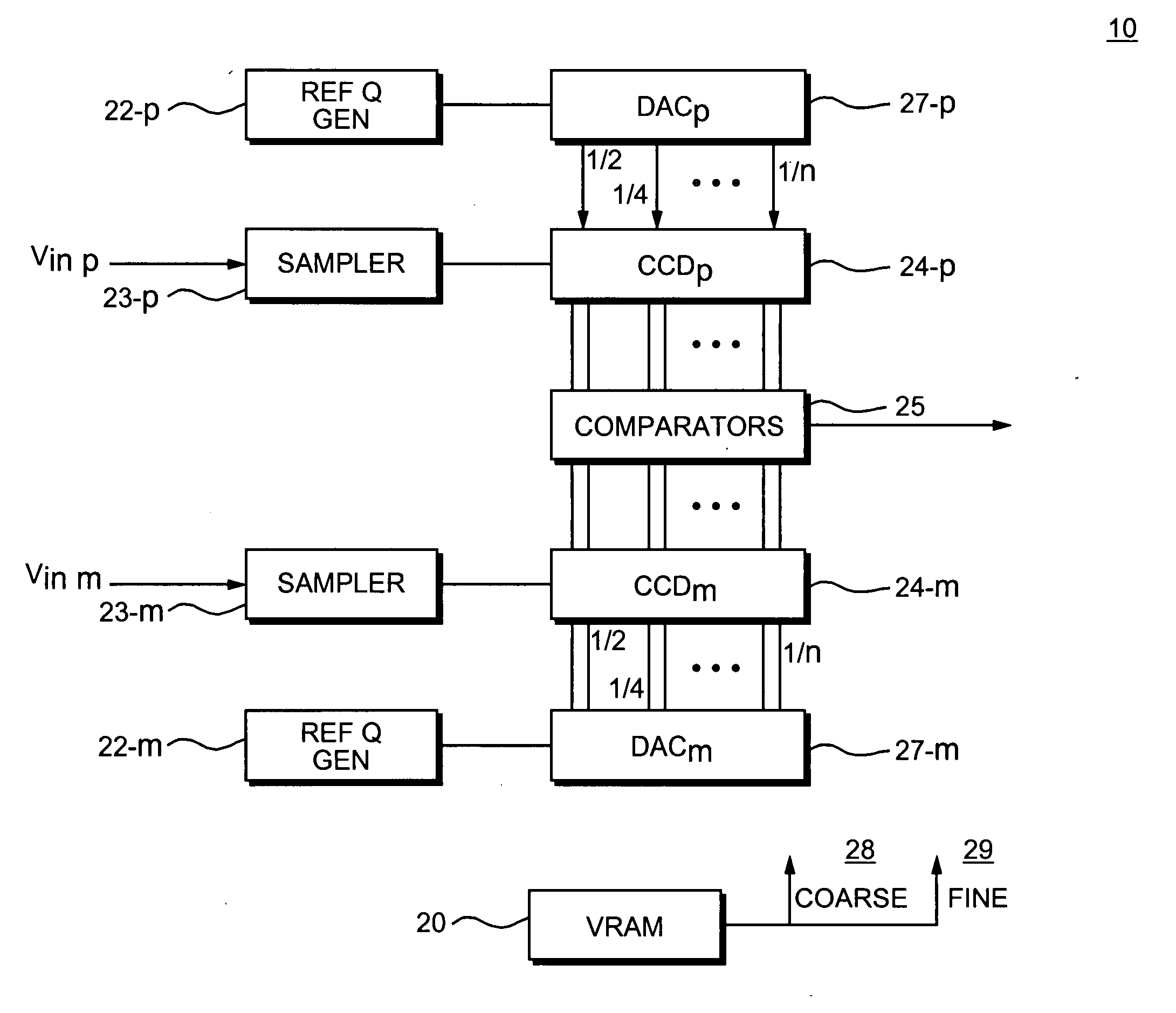
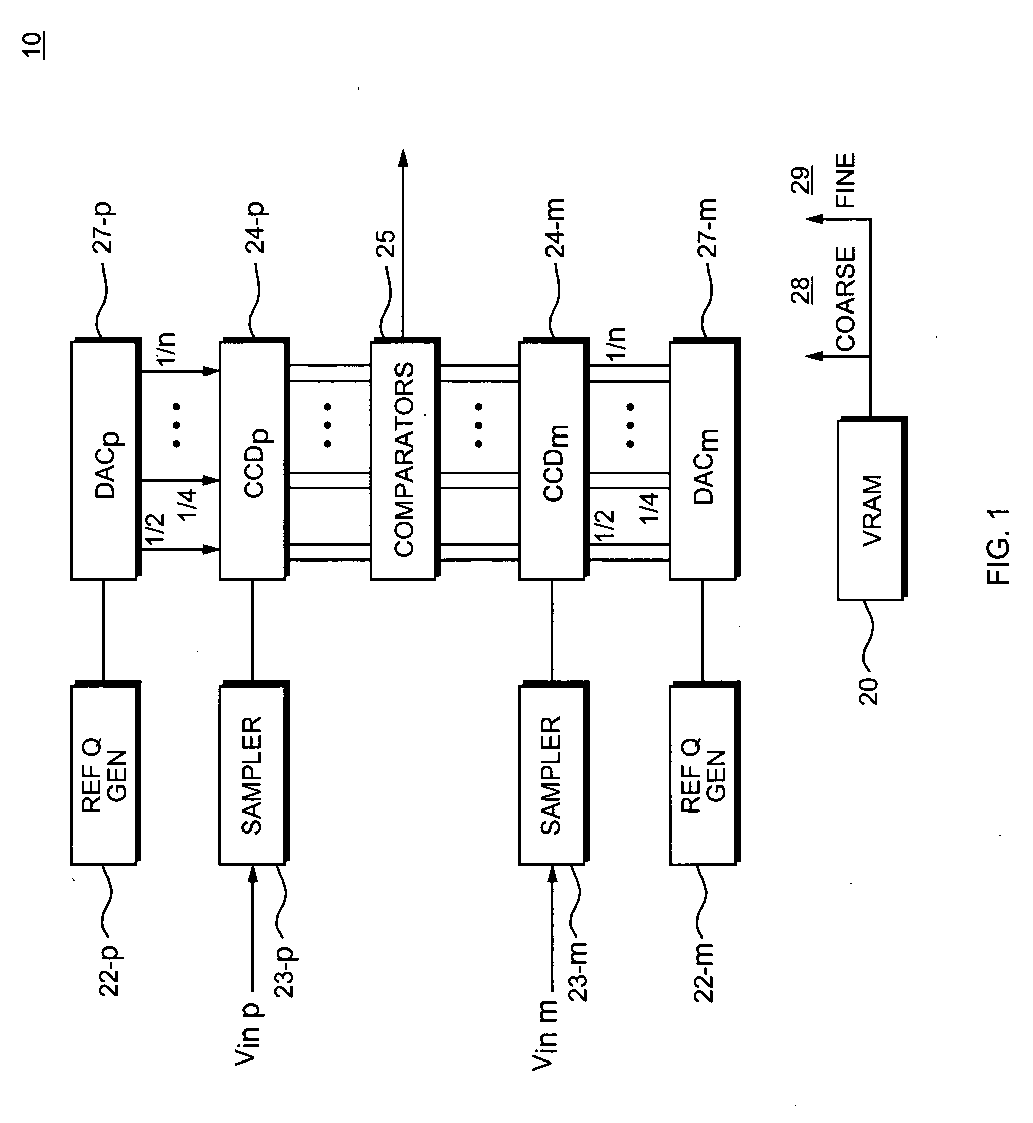
[0020]FIG. 1 is a block diagram of a device 10 that may use a Voltage Random Access Memory (VRAM) 20 according to the present invention. The illustrated device 10 is arranged as a Charge to Digital Converter (QDC). It should be understood, however, that the VRAM 20 can be used in any other application circuit where multiple analog voltages must be produced in parallel from digital inputs.

[0021] This particular QDC 10 is a so-called successive approximation type converter that uses a number of charge storage stages arranged as a serial pipeline register. In the illustrated circuit there are actually two pipelines 24-p, 24-m (a “plus” pipeline and a “minus” pipeline”) that carry charges as complimentary charge pairs. A reference charge generator 22-p, 22-m, input sampler 23-p, 23-m, and digital to analog converter (DAC) 27-p, 27-m are associated with each serial pipeline register 24-p, 24-m. A reference charge ge...


PUM


Abstract

An integrated circuit memory cell and voltage ladder design that adapts techniques typically applied to Static Random Access Memory (SRAM) circuits to implement a compact array of analog Voltage Random Access Memory (VRAM) locations. The memory cells in the VRAM each store a digital value that controls a corresponding switch. The switch couple a particular voltage from a set of voltages generated by the ladder, to be output when that location is enabled. Multiple analog output voltages are provided by simply providing additional rows of cells.

Description

RELATED APPLICATION(S) [0001] This application claims the benefit of U.S. Provisional Application No. 60 / 585,610, filed on Jul. 6, 2004, the entire teachings of which are incorporated herein by reference.BACKGROUND OF THE INVENTION [0002] Several different types of circuits require the generation of multiple analog output voltages in accordance with digital input signals. In such circuits it has been customary to implement this function using a separate digital to analog converter for each required output voltage. [0003] This approach is adequate when only a few analog voltages must be generated. However, certain types of circuits, such as charge to digital converters, may require generation of many such analog voltages. Even if integrated circuits are used to implement such circuits, the voltage generating function can occupy much space in a design. SUMMARY OF THE INVENTION [0004] The present invention is an integrated circuit memory cell and voltage ladder design to implement a co...

Claims


Application Information

Patent Timeline
IPC IPC(8): H03M7/00
CPCG11C7/02G11C7/16G11C11/412G11C11/413G11C27/00H03M1/785H03M1/662H03M1/682H03M1/76H03M1/765H03M1/1009H03M1/74H03M1/78
Inventor ANTHONY, MICHAEL P.KUSHNER, LAWRENCE J.
Owner KENET
Why Eureka
Try Eureka