Liquid crystal display device built-in finger printing device and method of manufacturing the same

Inactive Publication Date: 2006-01-26
SAMSUNG ELECTRONICS CO LTD
View PDF6 Cites 92 Cited by
  • Summary
  • Abstract
  • Description
  • Claims
  • Application Information

AI Technical Summary

Benefits of technology

[0025] Accordingly, when the fingerprint identification device having the sensor TFT is mounted on the TFT-LCD panel, the number of glass substrate can be reduced such that the manufacturing cost may be reduced. The liquid crystal display device according to the present invention requires only two glass substrates while the conventional liquid crystal display device requires three glass substrates. Particularly, when the liquid crystal display device is employed in the mobile devices such as the cellular phone, the thickness and total weight of the mobile device can be reduced.
[0026] In addition, the transmissivity of the TFT-LCD panel having the fingerprint identification device is increased according to the decrease of the n

Problems solved by technology

However, the optical fingerprint identification device is sensitive to distortion of images, cannot be easily miniaturized and is manufactured at a high cost.
Particularly, the optical fingerprint identification device is not suitable for mobile devices such as a cellular phone because the optical fingerprint identification device uses a plurality of lens such that the optical fingerprint identification device cannot be easily thinner and lighter.
However, the fingerprint identification device manufactured by

Method used


Image

  • Liquid crystal display device built-in finger printing device and method of manufacturing the same
  • Liquid crystal display device built-in finger printing device and method of manufacturing the same
  • Liquid crystal display device built-in finger printing device and method of manufacturing the same

Examples


Embodiment Construction

[0044] Hereinafter the preferred embodiment of the present invention will be described in detail with reference to the accompanying drawings.

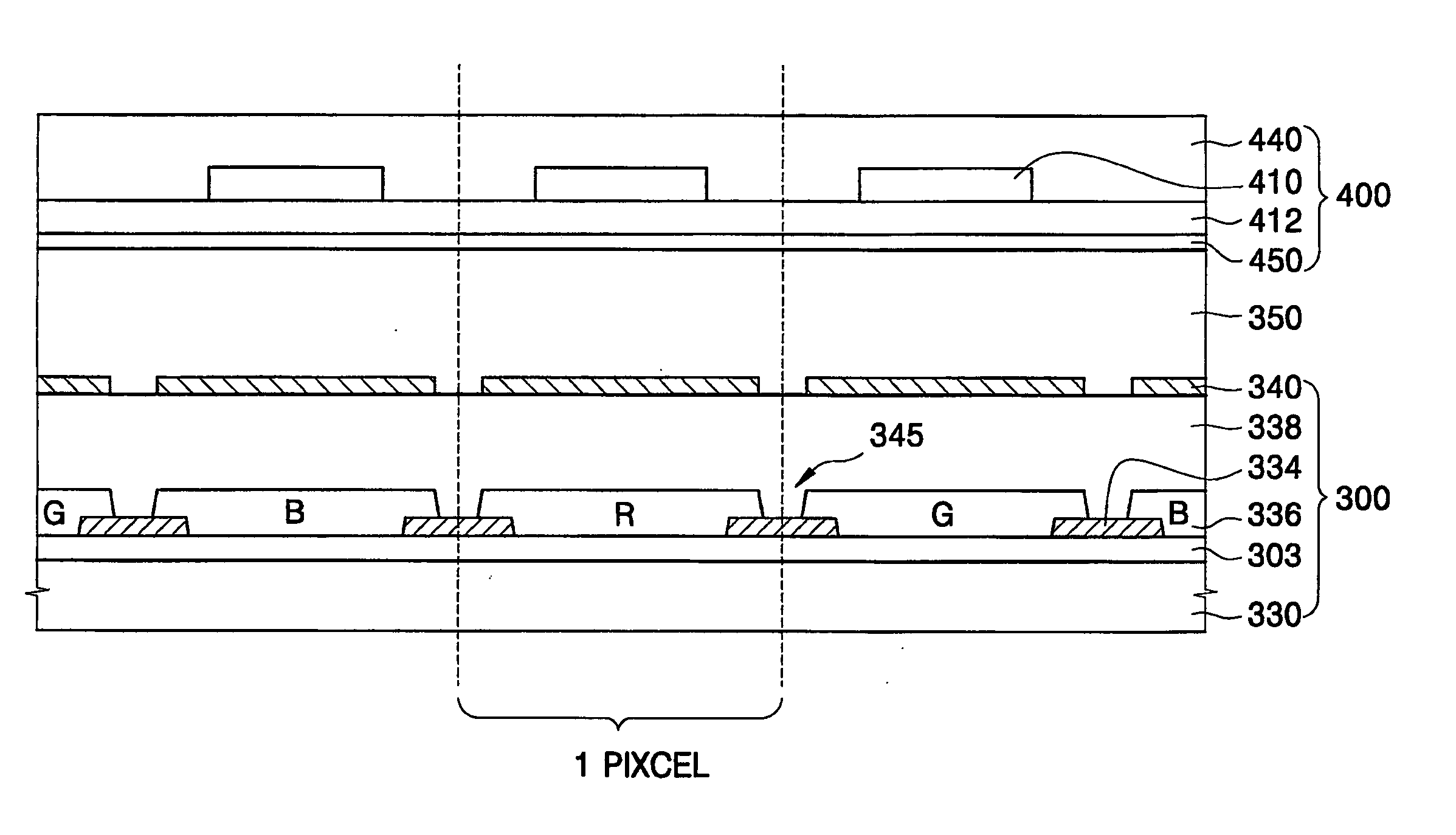
[0045]FIG. 3 is a cross-sectional view showing a color-filter-on-array structure of an a-Si TFT-LCD panel mounted with a TFT fingerprint identification substrate according to one exemplary embodiment of the present invention.

[0046] The color-filter-on-array structure is referred to as a structure in which color filters are formed on the TFT substrate to be aligned with thin film transistors of the TFT substrate. Namely, the color filters and the thin film transistors have a self-aligned structure. Accordingly, an aperture ratio of the TFT-LCD panel is increased. In addition, the color filters may be exactly aligned with the thin film transistors on the TFT substrate.

[0047] Referring to FIG. 3, the TFT fingerprint identification substrate 400 is attached to the TFT-LCD panel having the color-filter-on-array structure.

[0048] The TFT fingerpri...


PUM


Abstract

A liquid crystal display device having fingerprint identification device for enhancing aperture ratio and transmissivity of a TFT-LCD panel is disclosed. A fingerprint identification substrate (400) is attached to a TFT substrate (300). The TFI substrate has color-filter-on-array structure in which the color filters (336) and the thin film transistors can be eliminated, the aperture ratio is increased, and the quality of image display is enhanced. In addition, the transmissivity is increased according to the decrease of the number of glass substrate used in the liquid crystal display device, so that the sensitivity of fingerprint identification is enhanced.

Description

TECHNICAL FIELD [0001] The disclosure relates to a liquid crystal display device having a built-in fingerprint identification device and a method of manufacturing the liquid crystal display device. BACKGROUND ART [0002] An a-Si thin film transistor liquid crystal display (TFT-LCD) device is a flat panel display (FPD). The a-Si TFT-LCD device is used in a laptop computer, a monitor, a television set and a mobile phone. [0003] The a-Si TFT-LCD device displays an image by means of switch thin film transistors. In addition, the a-Si TFT-LCD device has a photosensitive property and is used as an optical sensor in the field of biometrics. [0004] In a personal authentication system, especially a fingerprint identification method using fingerprint identification devices is widely used because the fingerprint identification method may be accomplished at a low cost and has characteristics of high availability and high accuracy. [0005] The conventional fingerprint identification device may be ...

Claims


Application Information

Patent Timeline
IPC IPC(8): G02F1/136G02F1/13G02F1/133G06K9/00
CPCG02F1/13338G06K9/0004G02F2001/13312G02F1/13312G06V40/1318G02F1/13
Inventor SONG, JEAN-HOCHOI, JOON-HOOYANG, SUNG-HOONCHAI, CHONG-CHUL
Owner SAMSUNG ELECTRONICS CO LTD
Why Eureka
Try Eureka