
Optical waveguide and method of manufacture

a technology of optical waveguides and waveguides, applied in the direction of optical elements, crystal growth processes, instruments, etc., can solve the problems of limiting the application of optical signal processing, the characteristics of waveguide materials used are limited, and the modification of optical properties realized by the aforementioned application of heat, electric fields, magnetic fields or sound,

Inactive Publication Date: 2006-01-26
NIPPON TELEGRAPH & TELEPHONE CORP
View PDF18 Cites 2 Cited by
  • Summary
  • Abstract
  • Description
  • Claims
  • Application Information

AI Technical Summary

Benefits of technology

[0017] The present invention has been accomplished to overcome these problems and provide an optical waveguide and a method of manufacture thereof, the optical waveguide being capable of having a variety of characteristics not achievable with conventional devices and of forming a waveguide easily.
[0027] The Curie temperature varies depending on the composition x of KTaxNb1-xO3, and adding Li to KTaxNb1-xO3 can adjust its Curie temperature range.
[0031] The optical waveguide fabrication method of this invention requires depositing a thin film of KTaxNb1-xO3 with optical characteristics sufficient for light propagation, i.e., satisfactory crystal quality that produces such characteristics, and then forming the film into a predetermined structure at a predetermined location according to a design of the optical integrated circuit. Such an optical quality can be realized by a crystal epitaxial growth method. In a field of semiconductor crystal growth technology, an epitaxial growth method available that grows thin films having a high degree of lattice mismatch between a substrate and a thin film, as in the case of GaN-on-sapphire and GaAs-on-Si, is a micro-channel epitaxy (for example, T. Nishinaga and H. J. Scheel, “Advances in Superconductivity VIII,” ed. By H. Hayakawa and Y. Enomoto (Springer-Verlag, Tokyo, 1996) p. 33). This micro-channel epitaxy controls the thin film growth nucleation position by a groove formed on the upper surface of a seed layer on the substrate and improves the crystal quality of the thin film by the horizontal growth of the thin film from the nucleation position.
[0032] In this invention, since the nucleation position and the thin film growth direction can be controlled, when the crystal material has a strong crystal habit, it is possible to create a structure enclosed by the singular faces of the crystal material. The KTaxNb1-xO3 crystal material used in this invention has a cubic crystal structure and a strong crystal habit which is constructed by the {100} singular faces, so that a rectangular thin film enclosed by the {100} planes is likely to grow. In the process of growing a thin film, the growth nuclei on the substrate are generated starting from where the surface energy of the substrate is smallest. When there are holes or grooves on a planar substrate, the areas of the holes or grooves have side surfaces in addition to the bottom surfaces, increasing the number of contact surfaces with which the material supplied onto the substrate comes into contact. It is apparent also from the classical theory of crystal growth that an increase in the number of contact surfaces lowers the surface energy of the areas of the holes or grooves and thus the probability of crystal nuclei being generated in these areas becomes higher than in other planar areas.
[0036] That is, this invention is characterized by Li ions being diffused in the KTN crystal to form a core with a high refractive index. Li ions can be thermally diffused by substituting a K site and the KLTN crystal having the composition of K1-yLiyTa1-xNbxO3 also has a performance equal to or higher than that of the KTN crystal. Therefore, there is no possibility of characteristic degradation due to ion diffusion. Further, the relative index difference obtained by adding Li through thermal diffusion is 2% or higher, which is sufficient for the fabrication of a waveguide. This means that Li is an appropriate ion for forming waveguide. The melt containing LiNO3 used for diffusion has a low melting point of 261° C., which means that a stable melt can be obtained easily. This melt has a high water solubility so that, after the diffusion processing, it can be easily washed away with water. Thus, it has no adverse effects on the subsequent thermal diffusion processing in a gas.
[0037] As described above, the manufacture of a diffused waveguide using Li ions has-advantages that it can control the refractive index without degrading its characteristics and that the diffusion process using LiNO3 is simple and can perform diffusion at low temperatures.

Problems solved by technology

However, since the waveguide materials currently available are limited to SiO2, polymers, semiconductors and a small range of nonlinear crystals, the changing of the optical properties as realized by the method described above is greatly restricted by the characteristic of the waveguide material used, thus imposing limitations on the applicable optical signal processing.
The currently used waveguide materials, however, are limited to SiO2, polymers, semiconductors and a small range of nonlinear crystals.
Hence, the modification of optical properties as realized by the aforementioned application of heat, electric fields, magnetic fields or sound is greatly restricted by the characteristics of the waveguide material used.
The conventional optical ICs therefore have a problem that the applicable range of optical signal processing is very narrow.
Therefore, even in using the novel waveguide material KTaxNb1-xO3, the conventional technology has a problem that the waveguide fabrication process is complex.
Another problem is that, although the waveguide fabrication is essential in obtaining a desired performance, a technique to form waveguides in a KTN crystal has not yet been established.
As to K and Li compounds, there is not much information available about the materials which provide sufficient vapor pressures.
In the case of K in particular, no material has been known which is effective for use with the CVD method.
The essential reason for this is that alkali metal elements such as K and Li tend to be ionized easily and cannot easily be kept in a molecular state necessary for vaporization.

Method used


Image

  • Optical waveguide and method of manufacture
  • Optical waveguide and method of manufacture
  • Optical waveguide and method of manufacture

Examples


embodiment 1

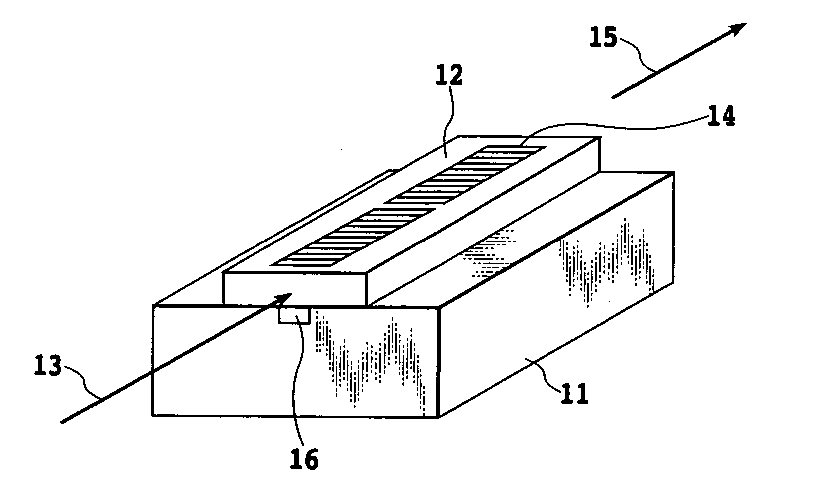
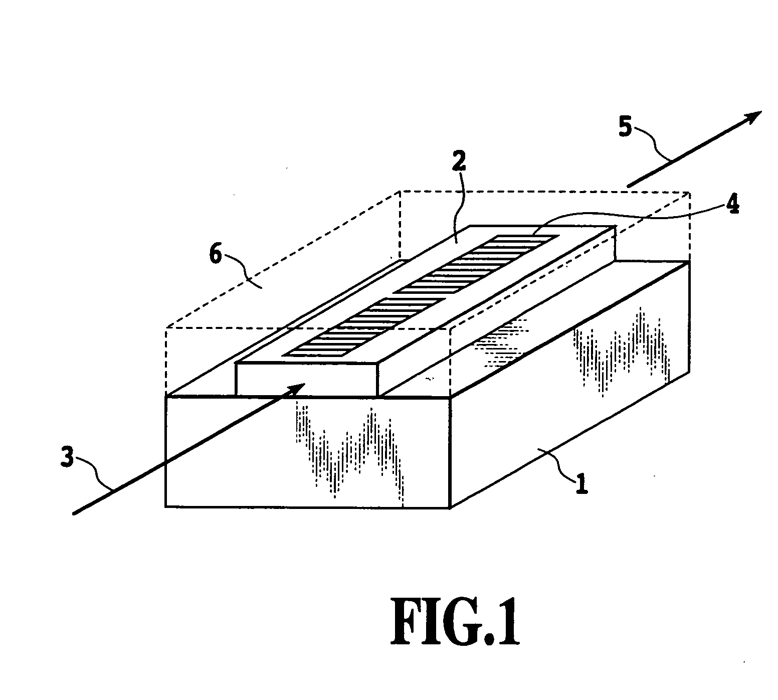
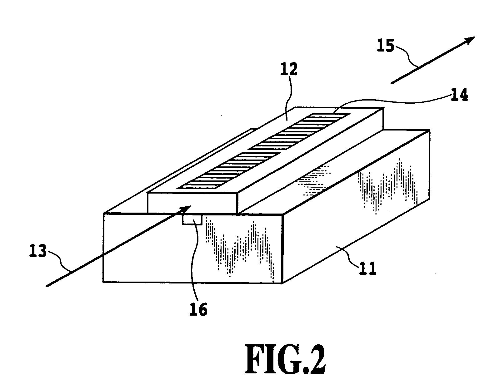
[0065]FIG. 1 is a perspective view showing the fabrication of an optical waveguide applying the present invention. A basic fabrication shown here as an example waveguide structure for explanation uses a ridge type optical waveguide as an optical waveguide and an electric field application from an electrode as an external field application mechanism. In the figure, reference number 1 represents a substrate that functions as an undercladding layer, 2 a waveguide layer having a refractive index higher than that of the substrate 1 and formed from a film of an optical functional material KTaxNb1-xO3 (03 an input optical signal, 4 an electrode, 5 an output optical signal, and 6 an overcladding layer (cover layer) covering the waveguide layer and having a refractive index lower than that of the waveguide layer KTaxNb1-xO3 film 2.

[0066] The input optical signal 3 is transmitted into the KTaxNb1-xO3 film 2. The KTaxNb1-xO3 film 2 changes its optical property by an external voltage signal ap...

embodiment 1-1

[0069] First, the manufacturing process 1 will be explained. In this embodiment, the liquid phase epitaxy capable of forming a single crystal film with high quality was adopted as the method of depositing a high quality KTaxNb1-xO3 film on the substrate 1. A KTaxNb1-xO3 (0≦x≦1) substrate, a MgO substrate, a MgAl2O4 substrate and a NdGaO3 substrate were used for the substrate 1. As the buffer layer (undercladding layer) were used a semiconductor Si substrate, a GaAs substrate and an InP substrate, which were formed by depositing such materials as SiO2, KTaxNb1-xO3 (0≦x≦1), MgO, MgAl2O4 and NdGaO3.

[0070] To prevent a possible contamination, the KTaxNb1-xO3 film 2 was formed by using potassium oxide and KTaxNb1-xO3 oxide as a solvent and a solute, respectively, and by using a self-flux method. As the potassium oxide solvent, a mixture of KVO3 and K2O (KVO3=30-70 molt) or K2CO3 carbonate was used. When a KTayNb1-yO3 (0≦y≦1) substrate was used, a material with x (01 are shown to have co...

embodiment 1-2

[0074] Next, the manufacturing process 2 will be explained. Photolithography was used to process the KTaxNb1-xO3 film to form a waveguide layer of a ridge type optical waveguide. A resist was applied to the thin film thus formed and was exposed and developed by using a mask for a 2 μm wide waveguide. The material was then etched by an ion milling method and the residual resist was removed, thereby forming a waveguide layer of the ridge type waveguide. The waveguide layer is nearly a 2 μm square and an observation of the side wall using a SEM (scanning electron microscope) found no significantly roughened surface.

[0075] The measurement of loss of this ridge type waveguide at a wavelength of 1.55 μm showed a loss value of 0.99 dB / cm, which means that the waveguide layer formed is good enough so that undulations of the surface as a result of processing can be neglected.


PUM

PropertyMeasurementUnit
Curie temperatureaaaaaaaaaa
dielectric constantaaaaaaaaaa

Abstract

An optical waveguide capable of having various characteristics and a method of manufacture thereof as well as a method of manufacturing a crystal film are provided. An optical functional material KTaxNb1-xO3 is used as an optical waveguide. The input optical signal is transmitted to the KTaxNb1-xO3 film. The KTaxNb1-xO3 film undergoes changes in optical property when an external voltage signal is applied to the electrode. Therefore, as it passes through the KTaxNb1-xO3 film, the input optical signal is modulated by the characteristic change. The modulated optical signal is taken out as an output optical signal.

Description

[0001] This application is based on Japanese Patent Application Nos. 2001-143570 filed May 14, 2001, 2001-143571 filed May 14, 2001, 2001-146560 filed May 16, 2001 and 2001-165283 filed May 31, 2001, the contents of which are incorporated hereinto by reference. BACKGROUND OF THE INVENTION [0002] 1. Field of the Invention [0003] The present invention relates to an optical waveguide and a method of manufacture thereof and more particularly to an optical waveguide for novel functional optical integrated circuits using an optical functional material KTaxNb1-xO3 as the optical waveguide and a method of manufacture thereof and also to a method of manufacturing a crystal film for use with optical communication devices. [0004] 2. Description of the Related Art [0005] Intensive research and development efforts are being made from a cost performance point of view to develop optical integrated circuits that integrate on a single substrate optical devices that perform emission, detection, modul...

Claims


Application Information

Patent Timeline
Patent Type & Authority Applications(United States)
IPC IPC(8): G02B6/10G02B6/12G02B6/132G02F1/00G02F1/035G02F1/355
CPCG02F1/3551Y10T29/49016G02B6/132G02B2006/12035G02B2006/12097G02B2006/121G02B2006/12109G02B2006/12142G02B2006/12164G02B2006/12173G02B2006/12176G02B2006/12178G02B2006/1218G02F1/0027G02F1/035Y10S117/918G02B6/13
Inventor SASAURA, MASAHIROFUJIURA, KAZUOENBUTSU, KOJIIMAI, TADAYUKIYAGI, SHOGOKURIHARA, TAKASHIABE, MAKOTOTOYODA, SEIJIKUBOTA, EISHI
Owner NIPPON TELEGRAPH & TELEPHONE CORP
Learn More