Light emitting display

a technology of light-emitting displays and display panels, applied in the field of light-emitting displays, can solve the problems of non-uniform line resistance of pixel power source lines, relatively heavy weight of crt displays, etc., and achieve the effect of uniform brightness

Active Publication Date: 2006-02-02
SAMSUNG DISPLAY CO LTD
View PDF10 Cites 51 Cited by
  • Summary
  • Abstract
  • Description
  • Claims
  • Application Information

AI Technical Summary

Benefits of technology

[0016] Accordingly, it is an aspect of the present invention to provide a light emitting display in which a power source line has a uniform voltage drop, thereby providing uniform brightness.
[0018] Other embodiments include a light emitting display including: a substrate; a pixel area including a plurality of pixels defined by scan lines and data lines formed on the substrate; a first power source line to supply the first power signal to each pixel on a first side of the pixel area; a second power source line to supply the first power signal to each pixel on a second side of the pixel area; a plurality of pixel power source lines having a first end electrically connected to the first power source line and a second end electrically connected to the second power source line to supply the first power signal from the first power source line and the second power source line to each pixel; and an impedance compensator connected to at least one of the first power source line and the second power source line to compensate for the difference in a voltage drop between the first power source line and the second power source line.

Problems solved by technology

Recently, various flat panel displays have been developed to replace cathode ray tube (CRT) displays, because CRT displays are relatively heavy and bulky.
However, in the conventional light emitting display, the pixel power source lines VDD that are commonly connected to the first power source line 50 are different in length from one another, so that the line resistance of the pixel power source lines is non-uniform, thereby supplying the power signal with differences in voltage drop (IR drop) to the respective pixels 21.

Method used


Image

  • Light emitting display
  • Light emitting display
  • Light emitting display

Examples


first embodiment

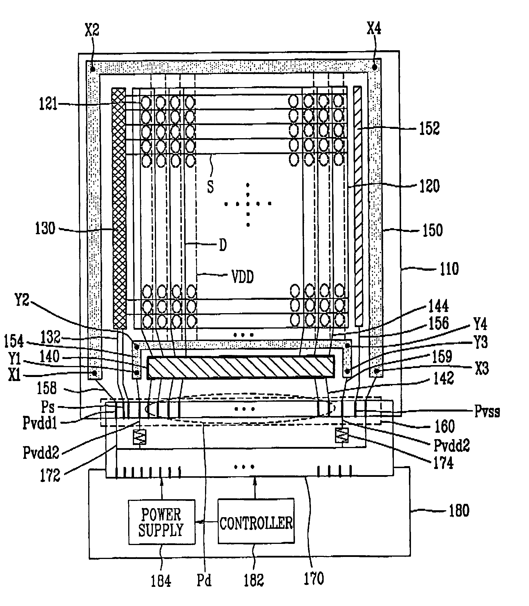
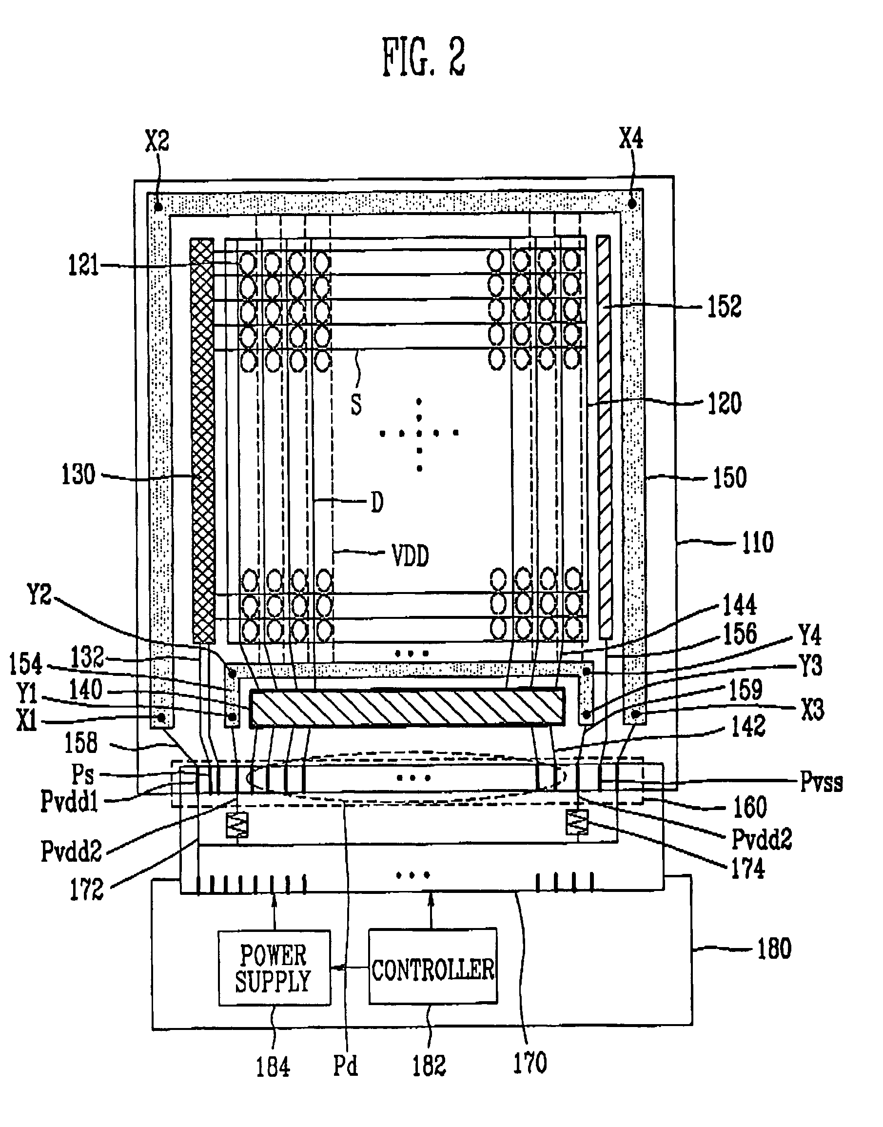
[0038]FIG. 2 is a view of a light emitting display according to the present invention.

[0039] Referring to FIG. 2, a light emitting display according to the first embodiment of the present invention includes: a substrate 110; a pixel area 120 including a plurality of pixels 121, which are defined by data lines D and scan lines S formed on the substrate 110, a light emitting device; a pixel circuit for controlling the emission of light; a first power source line 150 placed on a first side of the pixel area 120 and supplying a first power signal to the pixel area 120; a second power source line 154 placed on a second side of the pixel area 120 and supplying the first power signal to the pixel area 120; a plurality of power source lines VDD electrically connected to both the first power source line 150 and the second power source line 154 and supplying the first power signal to each pixel 121; a second power source line 152 supplying a second power signal to the plurality of pixels 121;...

second embodiment

[0063]FIG. 4 is a view of a light emitting display according to the present invention.

[0064] Referring to FIG. 4, the light emitting display according to the second embodiment of the present invention has the same configuration as that of the first embodiment except the placement of the data driver 140 for supplying a data signal to a data line D of a pixel area 120 has been moved.

[0065] The data driver 140 of the light emitting display according to the second embodiment of the present invention can be mounted on an FPC 170 connected to a substrate 110. Thus, the data driver 140 is electrically connected to the data line D of the pixel area 120 through a pad hub 160 of the substrate 110, thereby supplying the data signal. Alternatively, the data driver 140 may be provided on a chip-on-board that is mounted on a printed circuit board (PCB), may be directly mounted as a chip-on-film, or may be mounted on a general film-type connecting device employed in a tape carrier package, as wel...

third embodiment

[0066]FIG. 5 is a view of a light emitting display according to the present invention.

[0067] Referring to FIG. 5, the light emitting display according to the third embodiment of the present invention includes a substrate 210, a pixel area 220 including a plurality of pixels 221 which are arranged in areas defined by data lines D, scan lines S, and pixel power source lines VDD formed on the substrate 210, a scan driver 230, a data driver 240, a first power source line 250 having a first line width W1, a second power source line 254 having a second line width W2, a second power source line 252, and a pad hub 260.

[0068] The scan driver 230 is electrically connected to a first set of pads Ps on the pad hub 260 through the scan control signal line 232. The scan driver 230 generates a scan signal along the scan control signal line 232, and transmits the scan signal to the scan lines S of the pixel area 220 in sequence. The scan driver 230 includes a plurality of shift registers to genera...


PUM


Abstract

A light emitting display includes a substrate, a pixel area, a first power source line to supply a first power signal to each pixel on a first side of the pixel area, a second power source line to supply the first power signal to each pixel on a second side of the pixel area, and an impedance compensator for compensating a difference in a voltage drop between the first power source line and the second power source line. A voltage drop caused by line resistance that depends on the length of the first and second power source line that supply the first power signal to a lower and upper side of a pixel area, respectively, is equalized, thereby minimizing the voltage drop of the first power signal supplied to all pixels, and minimizing non-uniformity of brightness due to the voltage drop differences at each pixel.

Description

CROSS-REFERENCE TO RELATED APPLICATIONS [0001] This application claims priority to and the benefit of Korean Patent Application Nos. 10-2004-0059020 and 10-2004-0059021, filed on Jul. 28, 2004, in the Korean Intellectual Property Office, the entire contents of which is incorporated herein by reference. BACKGROUND [0002] 1. Field of the Invention [0003] The present invention relates to a light emitting display, and more particularly, to a light emitting display in which a power supply line has a uniform voltage drop, thereby providing uniform display brightness. [0004] 2. Discussion of Related Art [0005] Recently, various flat panel displays have been developed to replace cathode ray tube (CRT) displays, because CRT displays are relatively heavy and bulky. Flat panel displays include various types of light emitting display technologies including liquid crystal displays (LCDs), field emission displays (FEDs), plasma display panels (PDPs), and light emitting diode displays (LEDs). [000...

Claims


Application Information

Patent Timeline
Patent Type & Authority Applications(United States)
IPC IPC(8): G09G5/00
CPCG02F1/136286G09G3/32G09G2330/02G09G2320/0233G09G2320/0223
Inventor LEE, KYOUNG SOOEOM, KI MYEONGCHOI, JIN HYUN
Owner SAMSUNG DISPLAY CO LTD
Why Eureka
Try Eureka