Nonvolatile memory

a non-volatile memory, non-volatile technology, applied in static storage, digital storage, instruments, etc., can solve the problem that the reduction of write speed becomes inescapable, and achieve the effect of improving the write performance of memory information

Inactive Publication Date: 2006-02-02
RENESAS ELECTRONICS CORP
View PDF4 Cites 9 Cited by
  • Summary
  • Abstract
  • Description
  • Claims
  • Application Information

AI Technical Summary

Benefits of technology

[0029] An advantageous effect obtained by a representative one of the inventions disclosed in the present application will be explained in brief as follows:
[0030] Write performance for memory information can be improved in a nonvolatile memory.

Problems solved by technology

However, it has been found out by the present inventors that since the conductance of each control transistor must be reduced in the non cell-through write system, the resistance of each inversion layer increases, the write current is reduced small and correspondingly write variations also increase, eventually leading to the fear that a reduction in write speed will become inescapable.

Method used


Image

  • Nonvolatile memory
  • Nonvolatile memory
  • Nonvolatile memory

Examples


Embodiment Construction

>

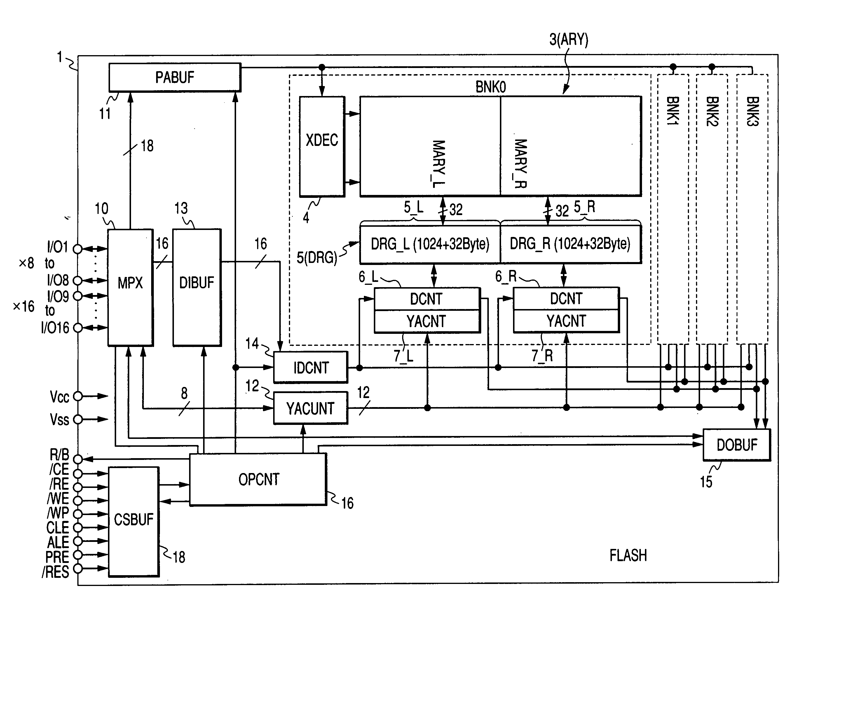
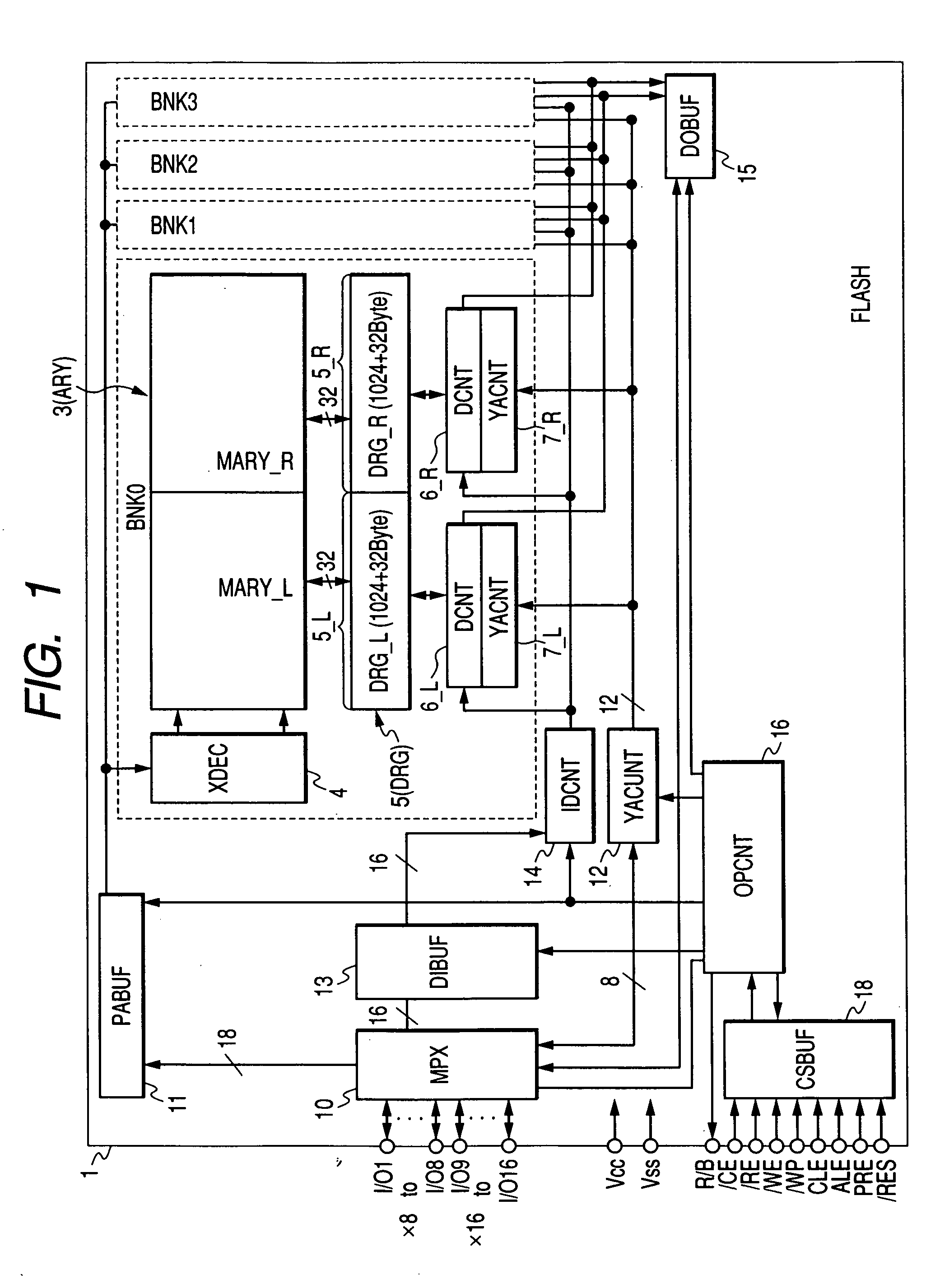
[0096] A flash memory is illustrated in FIG. 1. The flash memory 1 is formed over one semiconductor substrate such as monocrystalline silicon or the like.

[0097] Although not restricted in particular, the flash memory 1 has four memory banks BNK0 through BNK3. The respective memory banks BNK0 through BNK3 have configurations identical to one another and can be operated in parallel. The configuration of the memory bank BNK0 is typically illustrated in detail in the figure. Each of the memory banks BNK0 through BNK3 includes a flash memory array (ARY) 3, an X decoder (XDEC) 4, a data register (DRG) 5, data controllers (DCNT) 6_R and 6_L, and Y address controllers (YACNT) 7_R and 7_L.

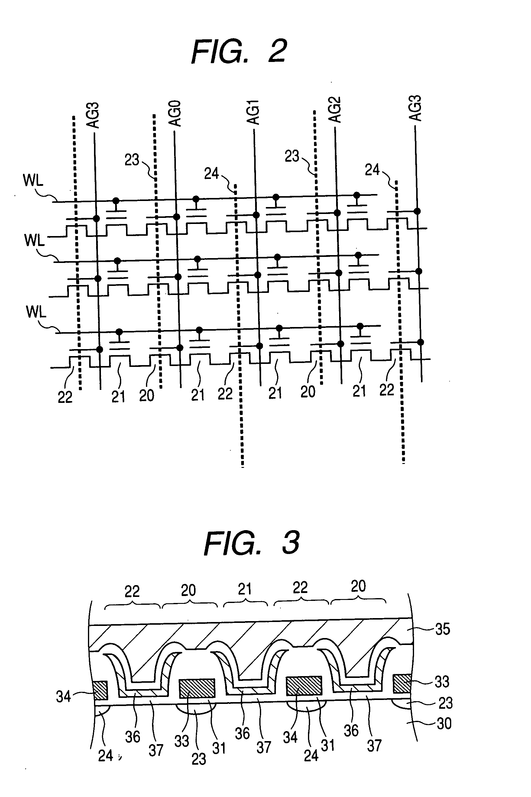
[0098] The memory array 3 has a large number of electrically erasable and programmable nonvolatile memory transistors. The details of the memory array will be described in detail later. However, the memory array is configured as a stacked gate structure in which memory gates are stacked on one another in...


PUM


Abstract

A nonvolatile memory includes circuits each having first control transistors, memory transistors, second control transistors and memory transistors repeatedly connected in series in sequence. Inversion layers are formed in the direction intersecting the serial direction with turning on of the control transistors. A selection circuit selects a connection of the inversion layer placed under the first control transistor and its corresponding read/write circuit. The control transistors placed on both sides adjacent to the memory transistor are turned on to perform reading. The first control transistors placed on both sides of the second control transistor as viewed from side to side are turned on to perform writing into the other of the right and left memory transistors via one of the right and left memory transistors. The selection circuit connects the read/write circuit and the inversion layer in such a manner that the same read/write circuit is used in reading and writing for the same memory transistor.

Description

CROSS-REFERENCE TO RELATED APPLICATION [0001] The present application claims priority from Japanese patent application No. 2004-225287 filed on Aug. 2, 2004, the content of which is hereby incorporated by reference into this application. BACKGROUND OF THE INVENTION [0002] The present invention relates to a programmable nonvolatile memory, and a technique effective if applied to, for example, an electrically programmable AND type flash memory. [0003] An AND type flash memory has been described in a patent document 1 (Japanese Unexamined Patent Publication No. 2004-152977). As one flash memory, there is shown a structure wherein diffusion regions are repeatedly parallel-formed over a semiconductor substrate, auxiliary electrodes are disposed among the respective diffusion regions through an oxide film interposed thereamong to form control transistors, and memory transistors each based on a charge storage region and a control gate are formed on the right and left sides of the auxiliary...

Claims


Application Information

Patent Timeline
Patent Type & Authority Applications(United States)
IPC IPC(8): G11C7/10
CPCG11C16/0425G11C16/0458G11C16/26G11C16/10G11C16/0491
Inventor KISHI, KOJIKURATA, HIDEAKINODA, SATOSHIJONO, YUSUKE
Owner RENESAS ELECTRONICS CORP
Why Eureka
Try Eureka