Light emitting diode display circuit with voltage drop compensation

a technology of light emitting diodes and display circuits, applied in static indicating devices, instruments, electroluminescent light sources, etc., can solve problems such as load (impedance), short-range (sr) uniformity, and voltage drop compensation

Inactive Publication Date: 2006-02-09
SAMSUNG DISPLAY CO LTD
View PDF6 Cites 69 Cited by
  • Summary
  • Abstract
  • Description
  • Claims
  • Application Information

AI Technical Summary

Benefits of technology

[0015] Accordingly, this invention provides a light emitting display that can compensate for the voltage drop difference between pixels, thereby making brightness uniform. This invention also

Problems solved by technology

However, in the conventional organic light emitting display, variation between the threshold voltages Vth of the TFTs occurs due to non-uniformity of the fabricating process.
Thus, the intensity of current applied to the organic light emitting diode varies, thereby causing problems with short-range (SR) uniformity.
However, in a case that the pixel power voltage line VDD is arranged in the horizontal direction as shown in FIG. 4, the load (impedance) increases as the number of transistors coupled to one horizontal pixel pow

Method used


Image

  • Light emitting diode display circuit with voltage drop compensation
  • Light emitting diode display circuit with voltage drop compensation
  • Light emitting diode display circuit with voltage drop compensation

Examples


first embodiment

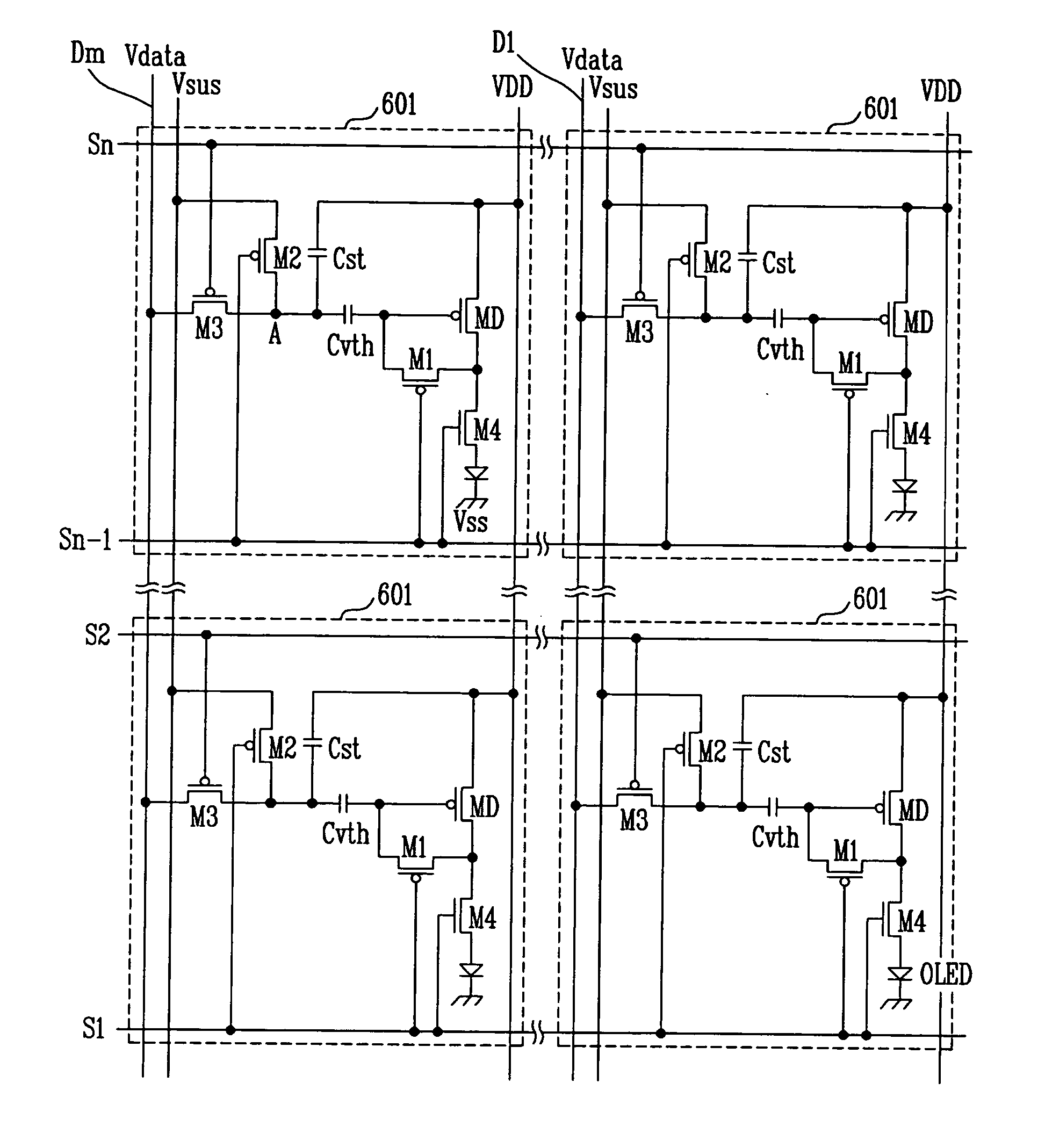
[0034] Referring to FIG. 5, a light emitting display according to the present invention includes a plurality of pixel circuits 601. As shown in FIG. 7, each pixel circuit 601 includes five transistors and two capacitors. In the example shown in FIG. 5, a pixel circuit 601 coupled to the (m-1)th data line Dm-1 and the (n-1)th scan line Sn-1 is shown among n×m pixel circuits 601. The light emitting display includes pixel circuits 601 having a second power source line Vsus to compensate voltage drop between pixels. In more detail, the pixel circuit 601 of the light emitting display includes a driving transistor MD, a first capacitor Cst, a second capacitor Cvth, a first switching device M1, a second switching device M2, a third switching device M3, and a fourth switching device M4. The first through fourth switching devices M1, M2, M3, M4 are formed from thin film transistors or TFT. Particularly, the fourth switching device M4 is formed from a dual gate type thin film transistor. With...

second embodiment

[0072]FIG. 9 is a circuit diagram of an organic light emitting display according to the present invention. For convenience of description, a pixel circuit coupled to the mth data line Dm and the nth scan line Sn will be described by way of example.

[0073] The pixel circuit 603 of the light emitting display according to the second embodiment is different from that according to the first embodiment in controlling a fourth transistor M4 through a separate signal line En. When the fourth transistor M4 is controlled through the separate signal line En, the fourth transistor M4 may have a p-type or an n-type channel without affecting the circuit. Also, in this case, an emission period of the pixel circuit 603 can be controlled independently of a selection period of the first scan line Sn-1.

[0074] Thus, according to this second embodiment, variation between the first power voltages VDD supplied to the respective pixels 603 due to voltage drop is compensated using the second power voltage V...


PUM


Abstract

A light emitting display having a pixel circuit for compensating driving voltage variation between pixels due to voltage drop in the voltage supply line. The light emitting display includes pixels, data lines extending in a first direction, through which a data signal is supplied to the pixels, scan lines extending in a second direction crossing the first direction, through which a selection signal is supplied to the pixels, a first power source line supplying driving voltage to the pixels, and a second power source line along the first direction supplying a compensating voltage to the pixels. The compensating voltage compensates for the drop of driving voltage across pixels that can cause non-uniformity in brightness of the display.

Description

CROSS-REFERENCE TO RELATED APPLICATION [0001] This application claims priority to and the benefit of Korean Patent Application No. 200449718, filed on Jun. 29, 2004, in the Korean Intellectual Property Office, the entire content of which is incorporated herein by reference. BACKGROUND [0002] 1. Field of the Invention [0003] The present invention relates to a light emitting display, and more particularly, to a light emitting display having an improved layout structure for compensating voltage drop difference between pixels. [0004] 2. Discussion of Related Art [0005] Generally, an organic light emitting display uses an organic light emitting diode made of fluorescent or electrically excitable phosphorous organic compounds. The organic light emitting diode emits light based on the supplied voltage or current. Further, the organic light emitting diode has a laminated structure including an anode, an organic thin film, and a cathode. The organic thin film is made of organic compounds. Fu...

Claims


Application Information

Patent Timeline
IPC IPC(8): G09G3/30H05B44/00
CPCG09G3/3233G09G2300/0819G09G2300/0852G09G2300/0861H01L27/3297G09G2320/043G09G2330/02H01L27/3244G09G2320/0223H10K59/12H10K59/131H01L27/124G09G2300/043G09G2320/0233G09G2320/0209
Inventor KIM, KEUM NAM
Owner SAMSUNG DISPLAY CO LTD
Why Eureka
Try Eureka