P-channel electrically alterable non-volatile memory cell

a non-volatile memory cell, electrically alterable technology, applied in the direction of solid-state devices, semiconductor devices, instruments, etc., can solve the problems of introducing cell disturb, charge leakage and retention failure, and memory cells disclosed in prior art are believed to suffer from high field induced silc issues, etc., to improve electrically alterable memory cells and operation methods.

Inactive Publication Date: 2006-02-16
MARVELL INT LTD
View PDF8 Cites 24 Cited by
  • Summary
  • Abstract
  • Description
  • Claims
  • Application Information

AI Technical Summary

Benefits of technology

[0013] It is the object of the invention to provide an improved electrically alterable memory cell and operation methods.
[0014] Briefly, a preferred embodiment of the present invention is a nonvolatile memory device. A substrate of a semiconductor material is provided having a p-type conductivity. A well in the substrate is provided having an n-type conductivity. A source and a drain of p-type conductivity are formed in the well. A channel in the well is created in between the source and the drain. A charge storage region is disposed over and insulated from the channel by a storage insulator. A control gate is formed over and insulated from the charge storage region by a coupling insulator. An injector having a p-type region and an n-type region is formed next to the channel. The injector permits hole carriers be injected into the well, transporting through the channel through the storage insulator onto the charge storage region.
[0015] Briefly, another preferred embodiment of the present invention is a method operating the nonvolatile memory device. The method comprises the steps of applying a first voltage to the p-type region of the injector, applying a second voltage to the n-type region of the injector, applying a third voltage to at least one of the source and the drain to form an inversion layer in the channel, and applying a fourth voltage to the control gate. The second voltage is sufficiently more negative with respect to the first voltage. The third voltage is sufficiently more negative with respect to the second voltage, and the fourth voltage is sufficiently more negative with respect to the third voltage to permit holes from the injector transporting through the well through the channel through the storage insulator onto the charge storage region.
[0016] Briefly, another preferred embodiment of the present invention is methods programming and erasing the nonvolatile memory device. The method of programming the memory cell comprises the steps of applying a first voltage to the well, applying a second voltage to the source, applying a third voltage to the drain, and applying a fourth voltage to the control gate. The fourth voltage is sufficiently more positive with respect to the third voltage and sufficient more negative with respect to the first and the second voltages. The third voltage is sufficiently more negative with respect to the first voltage to inject electrons from the channel through the storage insulator onto the charge storage region. The method of erasing the memory cell comprises the steps of applying a fifth voltage to the p-type region of the injector, applying a sixth voltage to the n-type region of the injector, applying a seventh voltage to at least one of the source and the drain to form an inversion layer in the channel, and applying a eighth voltage to the control gate. The sixth voltage is sufficiently more negative with respect to the fifth voltage. The seventh voltage is sufficiently more negative with respect to the sixth voltage, and the eighth voltage is sufficiently more negative with respect to the seventh voltage to permit holes from the injector transporting through the well through the channel through the storage insulator onto the charge storage region.
[0017] Briefly, another preferred embodiment of the present invention is an electrically erasable and programmable nonvolatile memory array. The array comprises a substrate of semiconductor material of a p-type conductivity, a well of an n-type conductivity in the substrate, and a plurality of nonvolatile memory cells arranged in a rectangular array of rows and columns. Each of the plurality of nonvolatile memory cells comprises a source and a drain of the p-type conductivity formed in the well with a channel of the well defined therebetween, a charge storage region disposed over and insulated from the channel by a storage insulator, and a control gate formed over and insulated from the charge storage region by a coupling insulator. Each of the memory cells further comprises an injector having a p-type region and an n-type region formed next to the channel.

Problems solved by technology

This high field stress effect on the storage insulator results in charge leakage and retention failure even when memory cells are under a low field condition.
Therefore, the memory cell disclosed in prior art is believed suffered from high field induced SILC issue.
However, an additional disadvantage associated with this type of memory cell is that the BBHE program scheme can often introduce cell disturb problem in memory cells sharing a same drain junction.
The cell size thus can be undesirably enlarged.
Therefore, such cell thus is believed to have the disadvantage on larger cell size.

Method used


Image

  • P-channel electrically alterable non-volatile memory cell
  • P-channel electrically alterable non-volatile memory cell
  • P-channel electrically alterable non-volatile memory cell

Examples


Embodiment Construction

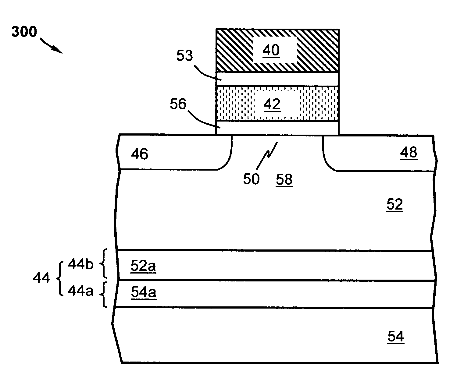
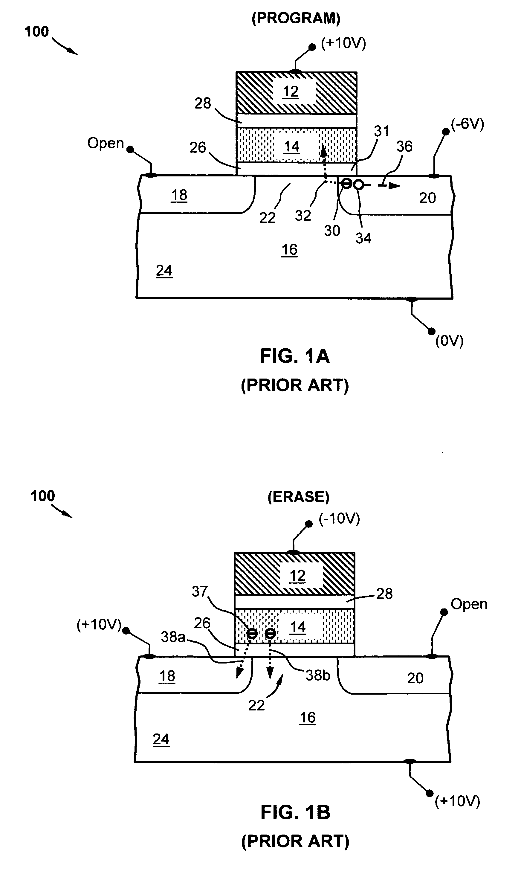
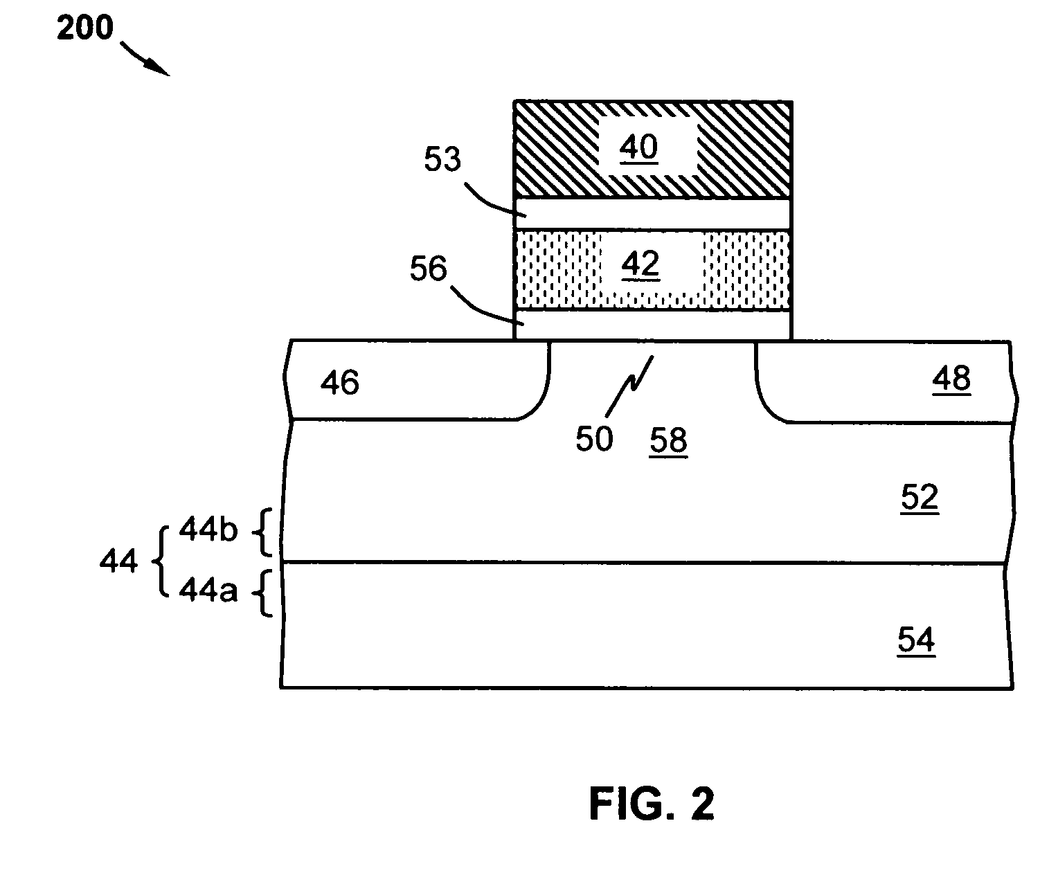
[0038] Embodiments of the present invention described in the following detailed description are directed at memory cell structures and operation methods. Those of ordinary skill in the art will realize that the detailed description is illustrative only and is not intended to restrict the scope of the claimed inventions in any way. Other embodiments of the present invention, beyond those embodiments described in the detailed descriptions, will readily suggest themselves to those of ordinary skill in the art having the benefit of this disclosure. Reference will now be made in detail to implementations of the present invention as illustrated in the accompanying drawings. Where appropriate, the same reference indicators will be used throughout the drawings and the following detailed description to refer to the same or similar parts.

[0039] In the interest of clarity, not all of the routine features of the implementations described herein are shown and described. It will, of course, be a...


PUM


Abstract

A nonvolatile memory cell is provided. The memory cell comprises a storage transistor and an injector in a semiconductor substrate of a p-type conductivity. The injector comprises a first region of the p-type conductivity and a second region of an n-type conductivity. The storage transistor comprises a source, a drain, a channel, a charge storage region, and a control gate. The source and the drain have the p-type conductivity and are formed in a well of the n-type conductivity in the substrate with the channel of the well defined therebetween. The charge storage region is disposed over and insulated from the channel by a first insulator. The control gate is disposed over and insulated from the charge storage region by a second insulator. Further provided are methods operating the memory cell, including means for injecting electrons from the channel through the first insulator onto the charge storage region and means for injecting holes from the injector through the well through the channel through the first insulator onto the charge storage region.

Description

RELATED APPLICATION [0001] This application is a Continuation-In-Part of U.S. patent application Ser. No. 10 / 919,555 filed on Aug. 16, 2004, entitled “ELECTRICALLY ALTERABLE NON-VOLATILE MEMORY CELL”.TECHNICAL FIELD [0002] The present invention deals with nonvolatile memory, and relates more specifically to Electrically Programmable Read Only Memories (EPROM) and Electrically Erasable and Programmable Read Only Memories (EEPROM). More particularly, the present invention relates to memory cell structure and method altering charge state of memory cells by employing mechanism injecting holes onto floating gate or charge storage sites of non-volatile memory cells for erase operation. BACKGROUND OF THE INVENTION [0003] Non-volatile semiconductor memory cells permitting charge storage capability are well known in the art. The charges stored thereon define the states of a memory cell. Typically, the states can be either two levels or more than two levels (for multi-level states storage). I...

Claims


Application Information

Patent Timeline
Patent Type & Authority Applications(United States)
IPC IPC(8): H01L29/788
CPCG11C16/0416G11C16/14H01L29/792H01L29/7885H01L29/42332
Inventor WANG, CHIH-HSIN
Owner MARVELL INT LTD
Why Eureka
Try Eureka