Silicon nanocrystal/erbium doped waveguide (SNEW) laser

a technology of erbium-doped waveguides and nanocrystals, which is applied in the direction of semiconductor lasers, laser details, electrical equipment, etc., can solve the problems of lack of suitable mirrors, difficult fabrication of non-standard materials, and high incompatibility with standard semiconductor microchip processes

Inactive Publication Date: 2006-02-23
UT BATTELLE LLC
View PDF3 Cites 33 Cited by
  • Summary
  • Abstract
  • Description
  • Claims
  • Application Information

AI Technical Summary

Benefits of technology

[0009] The structure for pumping can comprise a pair of electrodes sandwiching the active media. The rare earth can comprise Er and the laser cavity can be resonant from 1.52 to 1.57 microns. The subwavelength mirror can comprise a first and a second subwavelength mirror, the first and second subwavelength mirror disposed on respective ends of the laser cavity. In one embodiment, the first and second subwavelength mirrors comprise subwavelength resonant gratings, each grating comprising a plurality of periodically spaced high refractive index features disposed in the waveguide, the high refractive index features providing a refractive index higher than the refractive provided by the waveguide material. In another embodiment, the first and second subwavelength mirrors comprise photonic crystals, each photonic crystal having a plurality of low refractive index features in the waveguide, the low refractive index lower than the refractive provided by the waveguide material. In another embodiment, the subwavelength mirror can comprise a single distributed feedback structure (DFB), wherein light in the laser cavity is channeled toward a center of the cavity.

Problems solved by technology

The main reason why this integration has not yet occurred is due to the lack of any small CMOS compatible laser sources.
Such non-standard materials are difficult to fabricate and are highly incompatible with standard semiconductor microchip processes which are generally silicon-based.
However, several challenges including lack of suitable mirrors have generally prevented fabrication of laser cavities within optical waveguides.
A major drawback of Er doped amplifiers is their inability to be electronically pumped.
Another drawback of conventional Er-based amplifiers is the small gain coefficient provided.

Method used


Image

  • Silicon nanocrystal/erbium doped waveguide (SNEW) laser
  • Silicon nanocrystal/erbium doped waveguide (SNEW) laser
  • Silicon nanocrystal/erbium doped waveguide (SNEW) laser

Examples


Embodiment Construction

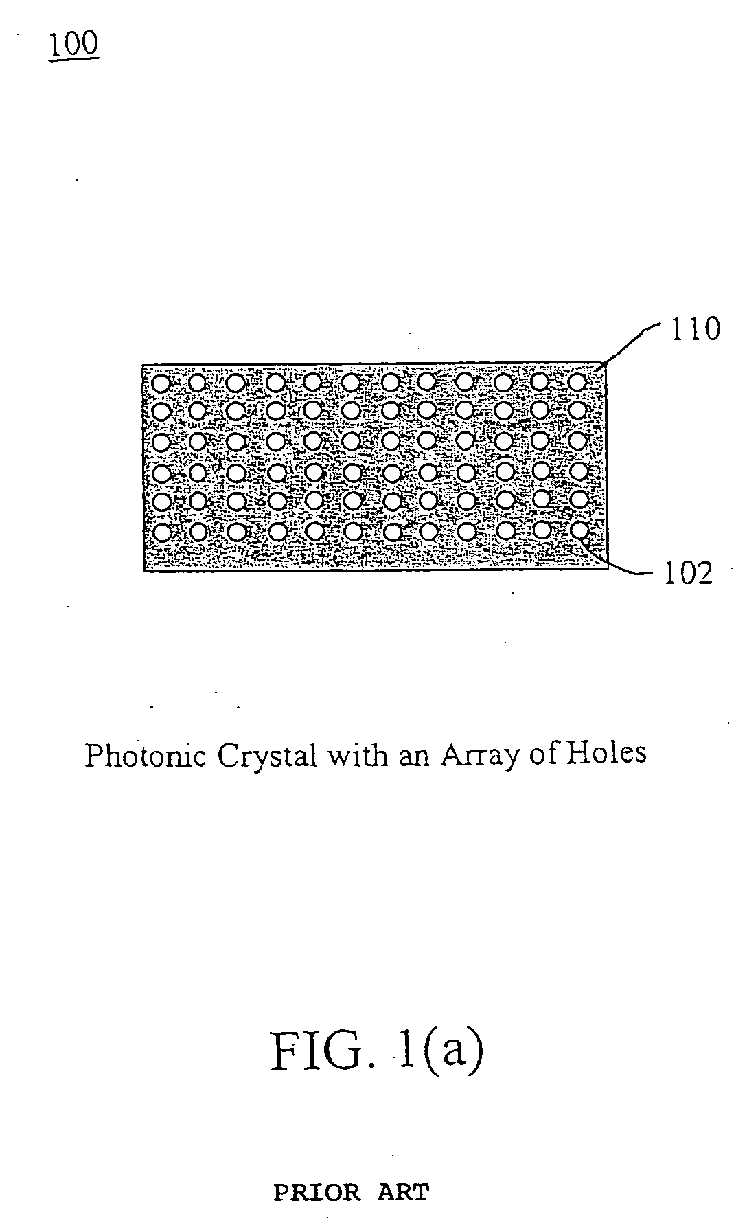
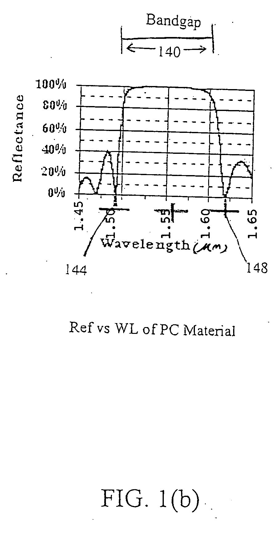
[0023] The present invention is related to U.S. patent application Ser. No. 10 / 315,578 ('578) filed on Dec. 10, 2002 entitled “NANOCRYSTAL WAVEGUIDE (NOW) LASER”, and is assigned to the same assignee as the present invention. '578 was published as published U.S. application No. 20040109483 on Jun. 10, 2004. '578 discloses a solid state laser including an optical waveguide and a laser cavity including at least one subwavelength mirror disposed in or on the optical waveguide. A plurality of semiconducting nanocrystals are disposed in the laser cavity. '578 is incorporated by reference into the current application in its entirety.

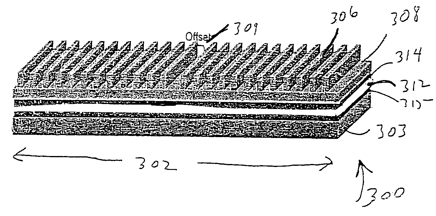
[0024] The present invention comprises a rare earth (RE)-doped solid-state integrated laser which includes an optical waveguide, and a laser cavity including at least one subwavelength mirror. The subwavelength mirror is disposed in or on the optical waveguide. The optical waveguide portion within the laser cavity includes active media comprising both an RE s...


PUM


Abstract

A rare earth-doped solid-state integrated laser which includes an optical waveguide, and a laser cavity including at least one subwavelength mirror. The subwavelength mirror is disposed in or on the optical waveguide. The optical waveguide portion within the laser cavity includes active media comprising both a rare earth and semiconducting atoms or compounds. A structure for pumping the semiconducting semiconducting atoms or compounds is provided, such as electrodes sandwiching the active media wherein the semiconducting atoms or compounds transfer energy obtained from the pumping to the rare earth, thus permitting the laser to laze.

Description

STATEMENT REGARDING FEDERALLY SPONSORED RESEARCH OR DEVELOPMENT [0001] The United States Government may have certain rights in this invention pursuant to Contract No. DE-AC05-00OR22725 between the United States Department of Energy and UT-Battelle, LLC.CROSS-REFERENCE TO RELATED APPLICATIONS [0002] Not applicable. FIELD OF THE INVENTION [0003] The invention relates to solid state lasers and optical amplifiers, more specifically optical waveguide cavity based lasers formed using subwavelength mirrors. BACKGROUND OF THE INVENTION [0004] Integration of optical components within semiconductor microchips has been a goal for many years. Such integration could create new and improved devices. The main reason why this integration has not yet occurred is due to the lack of any small CMOS compatible laser sources. Current solid-state lasers generally use gain media of non-standard III-V (or II-VI) materials, such as GaAlAs formed in a multiple quantum well configuration. Such non-standard mat...

Claims


Application Information

Patent Timeline
Patent Type & Authority Applications(United States)
IPC IPC(8): H01S5/00
CPCH01S3/0632H01S3/0635H01S3/169H01S3/1608H01S3/0637
Inventor SIMPSON, JOHN T.
Owner UT BATTELLE LLC
Why Eureka
Try Eureka