Display device and method for manufacturing the same
Active Publication Date: 2006-03-02
SEMICON ENERGY LAB CO LTD
View PDF43 Cites 77 Cited by
Summary
Abstract
Description
Claims
Application Information
AI Technical Summary
This helps you quickly interpret patents by identifying the three key elements:
Problems solved by technology
Method used
Benefits of technology
Benefits of technology
[0007] It is an object of the present invention to provide a method for manufacturing a display device that is highly reliable and has superior electric characteristics, at a low cost with high yield without complicating a process and an apparatus for manufacturing the display device.
[0008] According to the present invention, a step due to an opening in a contact is covered with an insulating layer to reduce the step, and is processed into a gentle shape. A wiring or the like is formed to be in contact with the insulating layer and thus the coverage of the wiring or the like is enhanced. In addition, deterioration of a light-emitting element due to contaminants such as water can be prevented by sealing a layer including an organic material that water permeability in a display device with a sealing material. Since the sealing material is formed in a portion of a driver circuit region in the display device, the frame margin of the display device can be narrowed.
[0012] According to the present invention, a highly reliable display device can be manufactured through a simplified process. Therefore, a display device that exhibits high-precision and high-quality images can be manufactured at a low cost with high yield.
Problems solved by technology
An EL element has a problem in that luminescence properties such as luminance or evenness of luminescence significantly deteriorate with time, as compared with an early period.
The low reliability is a factor in the limited practical application.
Method used
Image
Click on the blue label to locate the original text in one second.
Reading with bidirectional positioning of images and text.
Examples
embodiment mode 1
[0041] A method for forming a thin film transistor in Embodiment Mode 1 is described in detail with reference to FIGS. 1A to 6B.
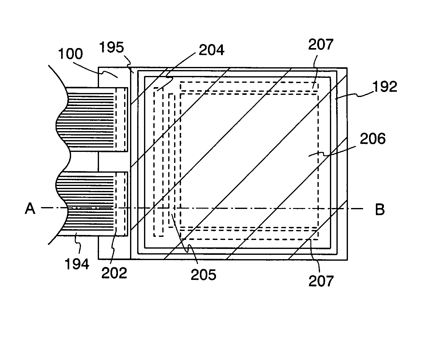
[0042] In addition, FIG. 16A shows a top view of a structure of a display panel according to the present invention. A pixel portion 2701 in which pixels 2702 are arranged in matrix, a scanning line input terminal 2703, and a signal line input terminal 2704 are formed over a substrate 2700 having an insulating surface. The number of pixels may be provided according to various standards. The number of pixels of XGA may be 1024×768×3 (RGB), that of UXGA may be 1600×1200×3 (RGB), and that of a full-speck high vision may be 1920×1080×3 (RGB).
[0043] The pixels 2702 are arranged in matrix by intersecting a scanning line extended from the scanning line input terminal 2703 with a signal line extended from the signal line input terminal 2704. Each pixel 2702 is provided with a switching element and a pixel electrode connected thereto. A typical example of the switc...
embodiment mode 2
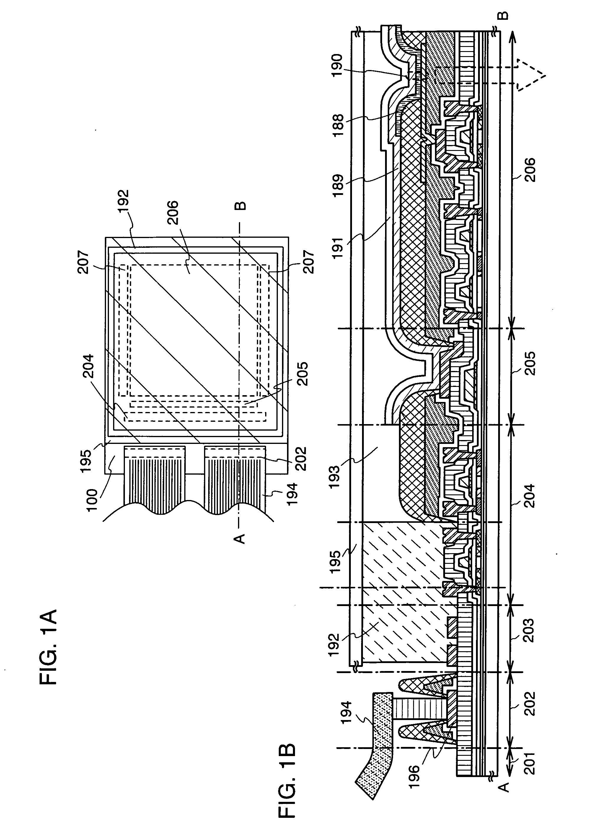
[0132] Embodiment Mode according to the present invention is described with reference to FIGS. 7A to 9. Embodiment Mode 2 describes an example in which a second interlayer insulating film is not formed in the display device manufactured in Embodiment Mode 1. Therefore, the description of the same portions and the portions having the same function is omitted.
[0133] As shown in Embodiment Mode 1, thin film transistors 173 to 176, a conductive layer 177, and insulating films 167 and 168 are formed over a substrate 100. A source or drain electrode layer to be connected to a source or drain region of a semiconductor layer is formed in each thin film transistor. A first electrode layer 395 is formed to be in contact with a source or drain electrode layer 172b in the thin film transistor 176 provided in a pixel region 206 (FIG. 7A).
[0134] The first electrode layer 395 serves as a pixel electrode, and may be formed from the same material in the same process as the first electrode layer 18...
embodiment mode 3
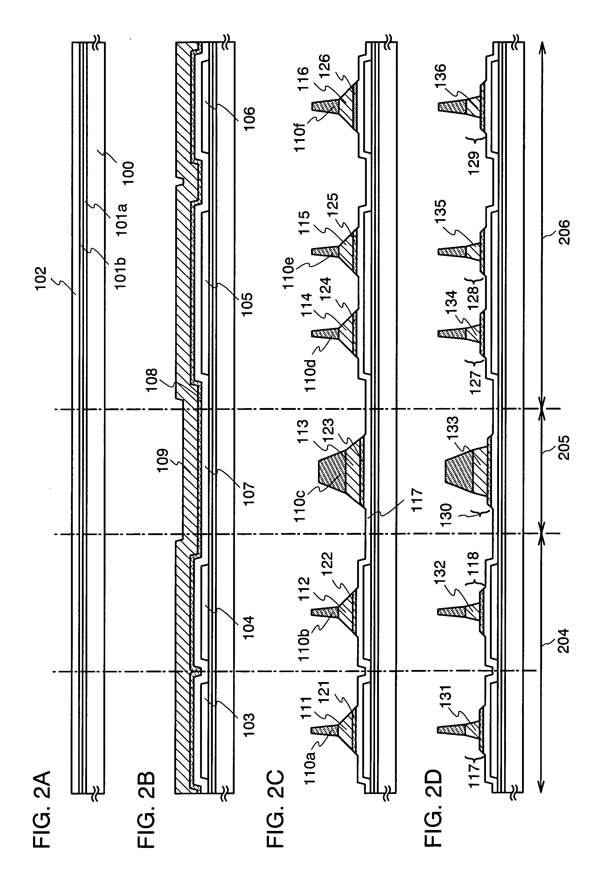
[0138] Embodiment Mode according to the present invention is described with reference to FIGS. 10A to 10C. Embodiment Mode 3 describes an example in which a gate electrode layer of a thin film transistor has a different structure in the display device manufactured in Embodiment Mode 1. Therefore, the description of the same portions and the portions having the same function is omitted.
[0139]FIGS. 10A to 10C show a display device that is being formed in a manufacturing process and corresponds to the display device shown in FIG. 4B described in Embodiment Mode 1.
[0140] In FIG. 10A, thin film transistors 273, 274 are formed in a peripheraldriver circuit region 214, a conductive layer 277 is formed in a connection region 215, and thin film transistors 275, 276 are formed in a pixel region 216. A gate electrode layer of a thin film transistor in FIG. 10A has a stacked structure of two conductive films, in which an upper gate electrode layer is patterned to have a width narrower than a...
PUM
Abstract
The present invention provides a method for manufacturing a highly reliable display device at a low cost with high yield. According to the present invention, a step due to an opening in a contact is covered with an insulating layer to reduce the step, and is processed into a gentle shape. A wiring or the like is formed to be in contact with the insulating layer and thus the coverage of the wiring or the like is enhanced. In addition, deterioration of a light-emitting element due to contaminants such as water can be prevented by sealing a layer including an organic material that has water permeability in a display device with a sealing material. Since the sealing material is formed in a portion of a driver circuit region in the display device, the frame margin of the display device can be narrowed.
Description
BACKGROUND OF THE INVENTION [0001] 1. Field of the Present Invention [0002] The present invention relates to a display device and a method for manufacturing the same. [0003] 2. Description of the Related Art [0004] An EL element has a problem in that luminescence properties such as luminance or evenness of luminescence significantly deteriorate with time, as compared with an early period. The low reliability is a factor in the limited practical application. [0005] As one factor of worsening reliability, water or oxygen which intrudes into the EL element from outside is given. [0006] Accordingly, a display device having a structure for preventing the deterioration of the EL element has been developed. In addition, there is a method by which a sealing material is formed over an insulator provided with an EL element, and an enclosed space surrounded by a covering material and the sealing material is filled with a filler made of resin or the like; therefore, the EL element is blocked of...
Claims
Application Information
Patent Timeline
Application Date:The date an application was filed.
Publication Date:The date a patent or application was officially published.
First Publication Date:The earliest publication date of a patent with the same application number.
Issue Date:Publication date of the patent grant document.
PCT Entry Date:The Entry date of PCT National Phase.
Estimated Expiry Date:The statutory expiry date of a patent right according to the Patent Law, and it is the longest term of protection that the patent right can achieve without the termination of the patent right due to other reasons(Term extension factor has been taken into account ).
Invalid Date:Actual expiry date is based on effective date or publication date of legal transaction data of invalid patent.

