Light emitting display and driving method including demultiplexer circuit

a technology of light emitting display and driving method, which is applied in the direction of electroluminescent light sources, static indicating devices, instruments, etc., can solve the problems of increasing the production cost of led and increasing production costs, and achieves uniform brightness, reduce production costs, and reduce output lines

Inactive Publication Date: 2006-03-02
SAMSUNG SDI CO LTD
View PDF16 Cites 45 Cited by
  • Summary
  • Abstract
  • Description
  • Claims
  • Application Information

AI Technical Summary

Benefits of technology

[0020] As described above, the present invention provides a LED and a driving method for the LED, in which a data signal supplied from one output line can be split and supplied to a plurality of second data lines, thereby decreasing the number of output lines and reducing the production cost. Further, the present invention provides a LED and a driving method for the LED, in which voltages corresponding to the data s

Problems solved by technology

Therefore, the data driver 20 includes a plurality of data integrated circuits so as to have m output lines, resulting in a problem of increased production cost.
Particularly, as

Method used


Image

  • Light emitting display and driving method including demultiplexer circuit
  • Light emitting display and driving method including demultiplexer circuit
  • Light emitting display and driving method including demultiplexer circuit

Examples


first embodiment

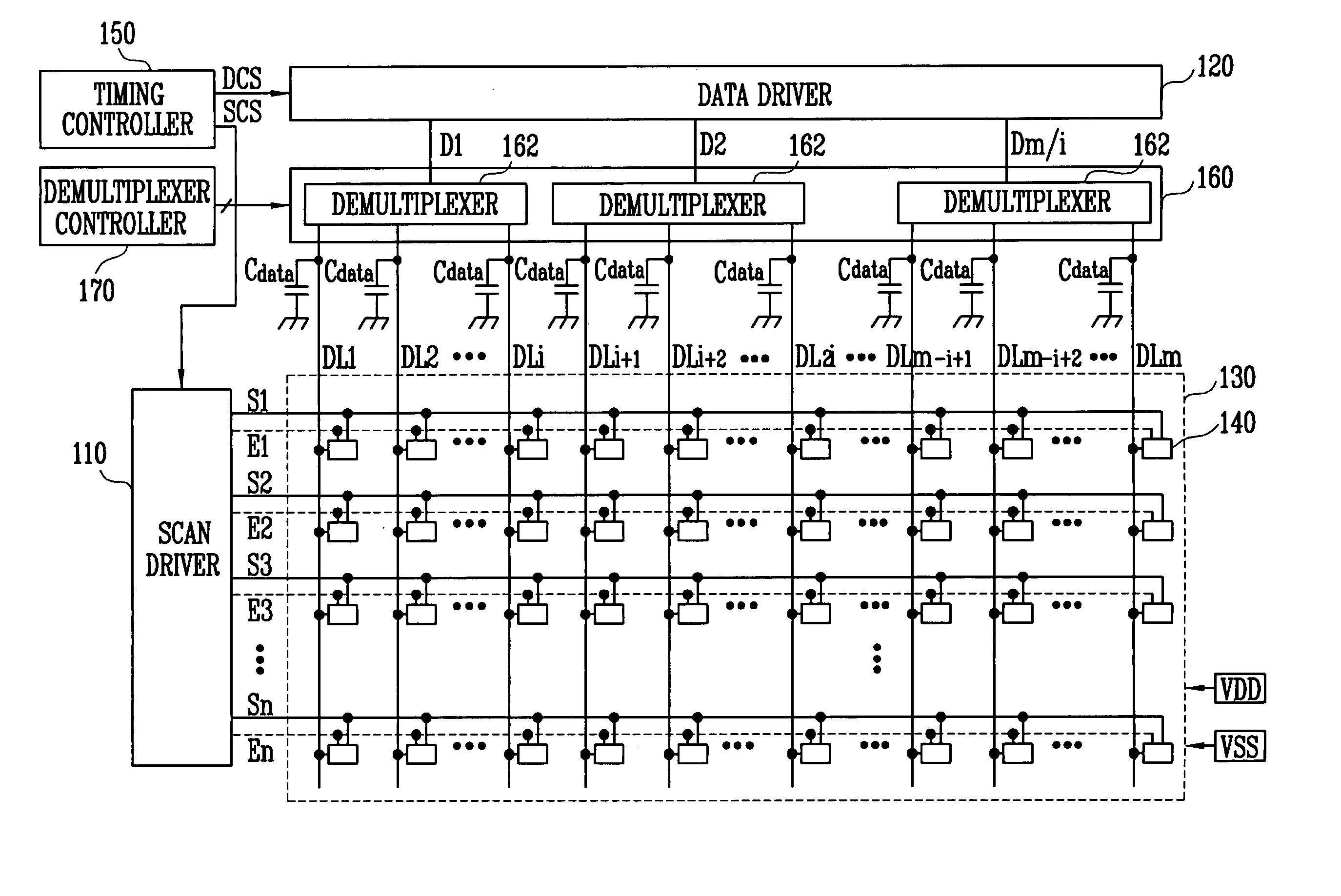
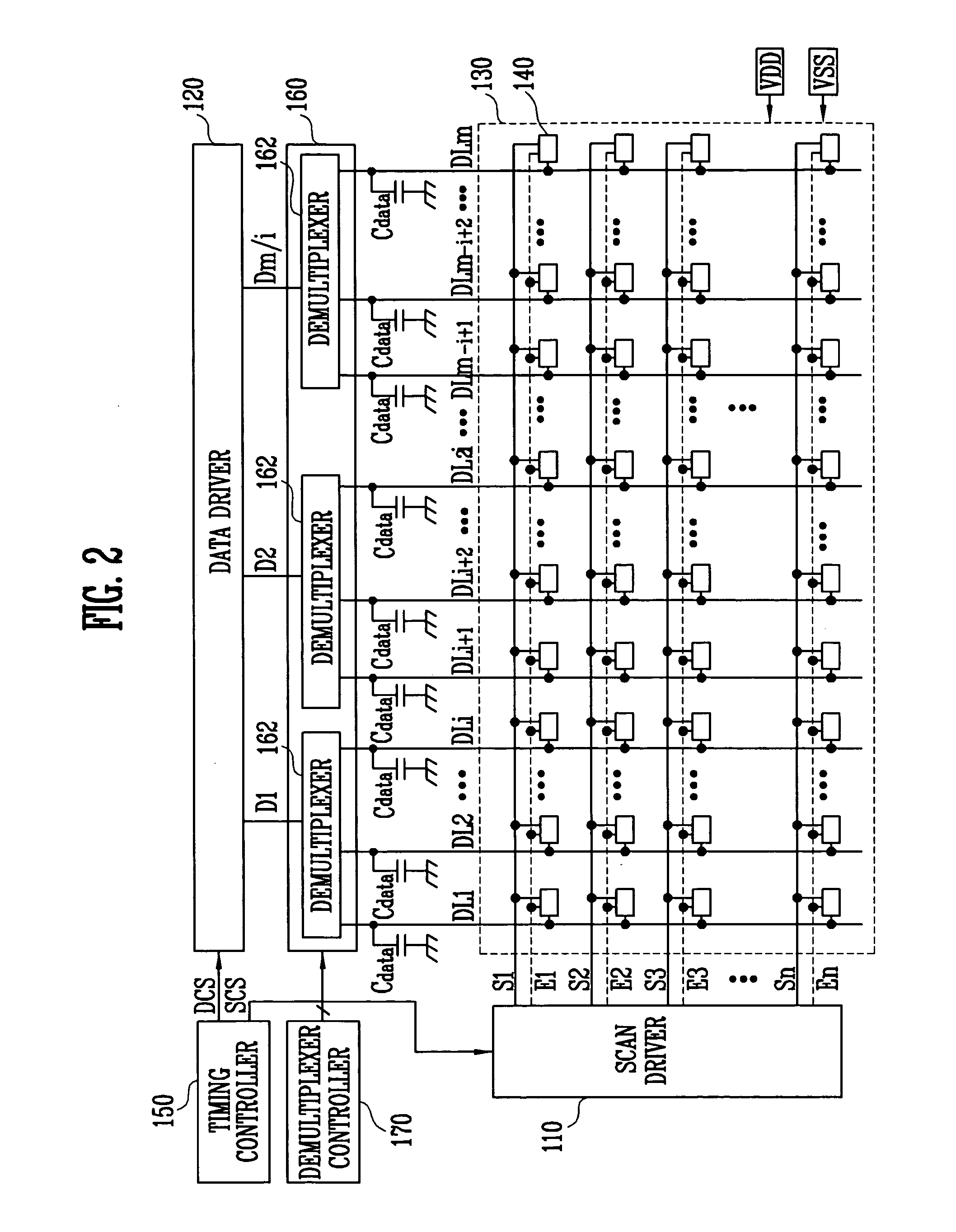
[0053]FIG. 6 is a circuit diagram showing connection between the demultiplexer 162 and the pixel 142 according to the present invention. In this example, one demultiplexer 162, where i is equal to 3, is coupled with three R, G, B, pixels 142R, 142G, 142B.

[0054] Referring now to FIGS. 4A and 6 to demonstrate the operation of the demultiplexer 162 and the pixel 140, first, the scan signal is transmitted to the (n−1)th scan line Sn−1 during the scan period in the one horizontal period. When the scan signal is transmitted to the (n−1)th scan line Sn−1, the sixth transistor M6 of each of the pixels 142R, 142G, 142B is turned on. As the sixth transistor M6 is turned on, the storage capacitor Cst and the gate terminal of the first transistor M1 are coupled to the (n−1)th scan line Sn−1. That is, when the scan signal is transmitted to the (n−1)th scan line Sn−1, the scan signal is supplied to the storage capacitor Cst and the gate terminal of the first transistor M1 provided in each of the ...

second embodiment

[0060]FIG. 7 is a circuit diagram of a pixel 140 provided in the LED according to the present invention. The circuit for a pixel 140 is not limited to the structure shown in this figure and may include at least one transistor capable of being used as a diode. Each pixel 140 includes a light emitting device OLED, and a pixel circuit 144 coupled to the second data line DL and to the scan lines and controlling and causing the light emitting device OLED to emit light.

[0061] The light emitting device OLED includes an anode electrode coupled to the pixel circuit 144, and a cathode electrode coupled to a second voltage VSS. The second voltage VSS is lower than a first voltage VDD applied to the pixel circuit 144. For example, ground voltage can be applied as the second voltage VSS. The light emitting device OLED emits light corresponding to current supplied from the pixel circuit 144. To emit light, the light emitting device OLED may include fluorescent and / or phosphorescent organic materi...


PUM


Abstract

A light emitting display and its driving method using a demultiplexer to reduce the number of output lines of a data driver. The light emitting display includes a scan driver supplying a scan signal to a scan line, a data driver having output lines and supplying data signals to the output lines, a demultiplexer in each output line and supplying the data signal from each one output line to a number of data lines, an image displaying part including pixels formed in regions defined by the scan and data lines, and a capacitor coupled to each data line to be charged with a voltage corresponding to the data signal supplied to the data line. With this configuration, the number of output lines required in the data driver is reduced. Further, the voltages charged in the data capacitors are supplied to the pixels simultaneously, thereby displaying an image with uniform brightness.

Description

CROSS-REFERENCE TO RELATED APPLICATION [0001] This application claims priority to and the benefit of Korean Patent Application No. 2004-67282, filed on Aug. 25, 2004, in the Korean Intellectual Property Office, the entire content of which is incorporated herein by reference. BACKGROUND [0002] 1. Field of the Invention [0003] The present invention relates to a light emitting display and a driving method thereof, and more particularly, to a light emitting display and a driving method thereof, in which the number of output lines provided in a data driver is reduced by using a demultiplexer. [0004] 2. Discussion of Related Art [0005] Recently, various flat panel displays have been developed, which are more desirable substitutes for a cathode ray tube (CRT) display because the CRT display is relatively heavy and bulky. The flat panel displays include liquid crystal displays (LCD), field emission displays (FED), plasma display panels (PDP), light emitting displays (LED), and the like. [00...

Claims


Application Information

Patent Timeline
IPC IPC(8): G09G3/32H05B44/00
CPCG09G3/3233G09G5/02G09G2300/0819G09G2300/0842G09G2320/043G09G2310/0251G09G2310/0262G09G2310/0297G09G2300/0861G09G3/30
Inventor KIM, YANG WAN
Owner SAMSUNG SDI CO LTD
Why Eureka
Try Eureka