

Prevention of photoresist scumming
a photoresist and scumming technology, applied in the field of microlithography, can solve the problems of small photoresist wavelength, acid generated during exposure diffuses into the underlying layer, and it is not possible to achieve sufficient acid to facilitate the removal of all exposed resists, etc., to achieve the effect of improving the pattern transfer
- Summary
- Abstract
- Description
- Claims
- Application Information
AI Technical Summary
Benefits of technology
Problems solved by technology
Method used
Image

Examples
Embodiment Construction
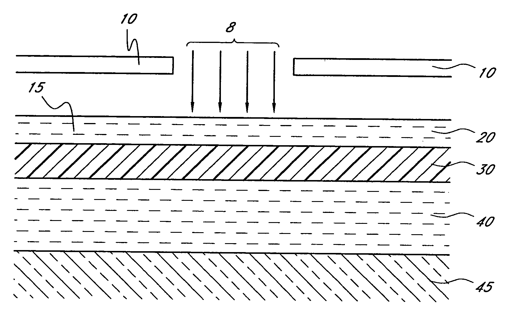
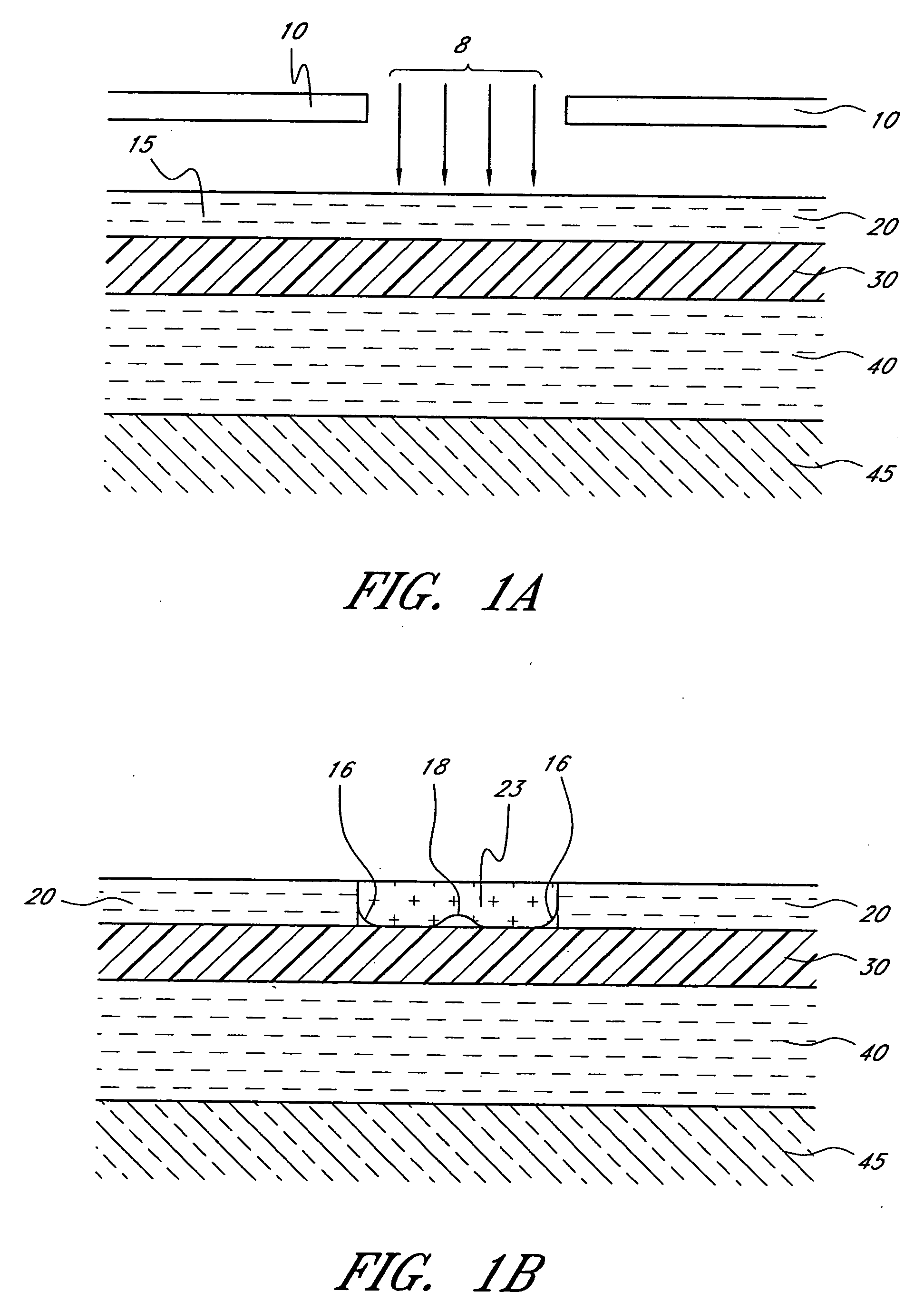
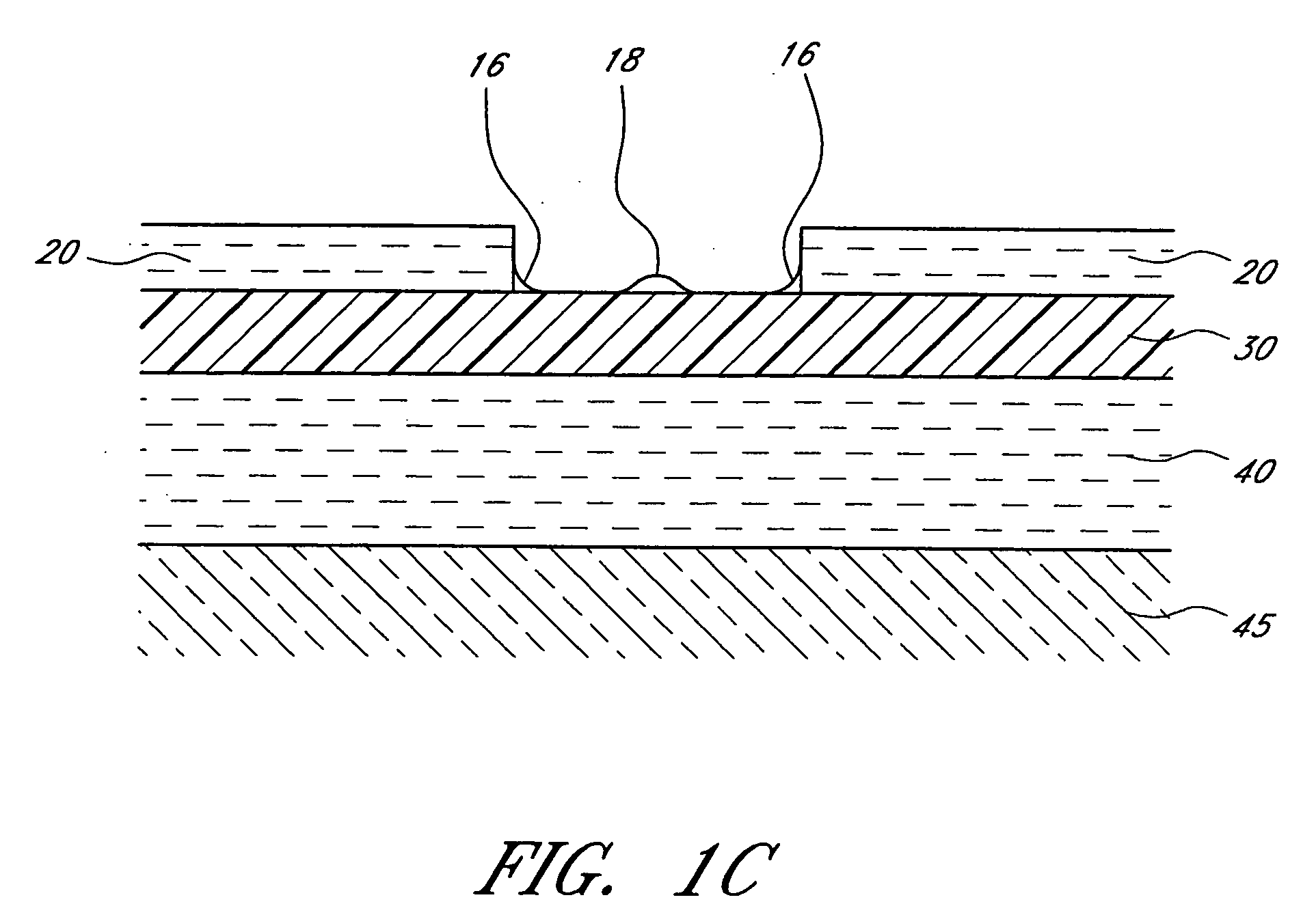
[0023] The significance of the problem of photoresist scumming and footing is growing because of the decreasing size of the resist and the circuits that are being patterned. Scumming, or resist remaining after development, is at least partially the result of resist that was not fully broken down by the acid generated in the resist. This scumming can cause footing and poorly formed features.
[0024]FIGS. 1A-1C illustrate a typical photoresist exposure and developing process and scumming effects. FIG. 1A shows a reticle 10 spaced above a photoresist layer 20. The photoresist 20 is over a first hard mask layer 30, a lower layer 40, and a substrate 45. The first hard mask layer 30, in this case an insulating underlayer such as an oxide, is directly beneath the resist 20. An illustrated lower layer 40 beneath the first hard mask layer 30 can be the substrate to be processed or an additional hard mask material. In the illustrated embodiment, the lower layer 40 comprises a layer of amorphou...
PUM
 Abstract
Description
Claims
Application Information