Semiconductor device having tin-based solder layer and method for manufacturing the same

Active Publication Date: 2006-03-09
DENSO CORP
View PDF7 Cites 18 Cited by
  • Summary
  • Abstract
  • Description
  • Claims
  • Application Information

AI Technical Summary

Benefits of technology

[0012] By using the tin-based solder layer and the minimum number of the metal layers, the backside of the substrate is solde

Problems solved by technology

Thus, the manufacturing process becomes simple and

Method used


Image

  • Semiconductor device having tin-based solder layer and method for manufacturing the same
  • Semiconductor device having tin-based solder layer and method for manufacturing the same
  • Semiconductor device having tin-based solder layer and method for manufacturing the same

Examples


first embodiment

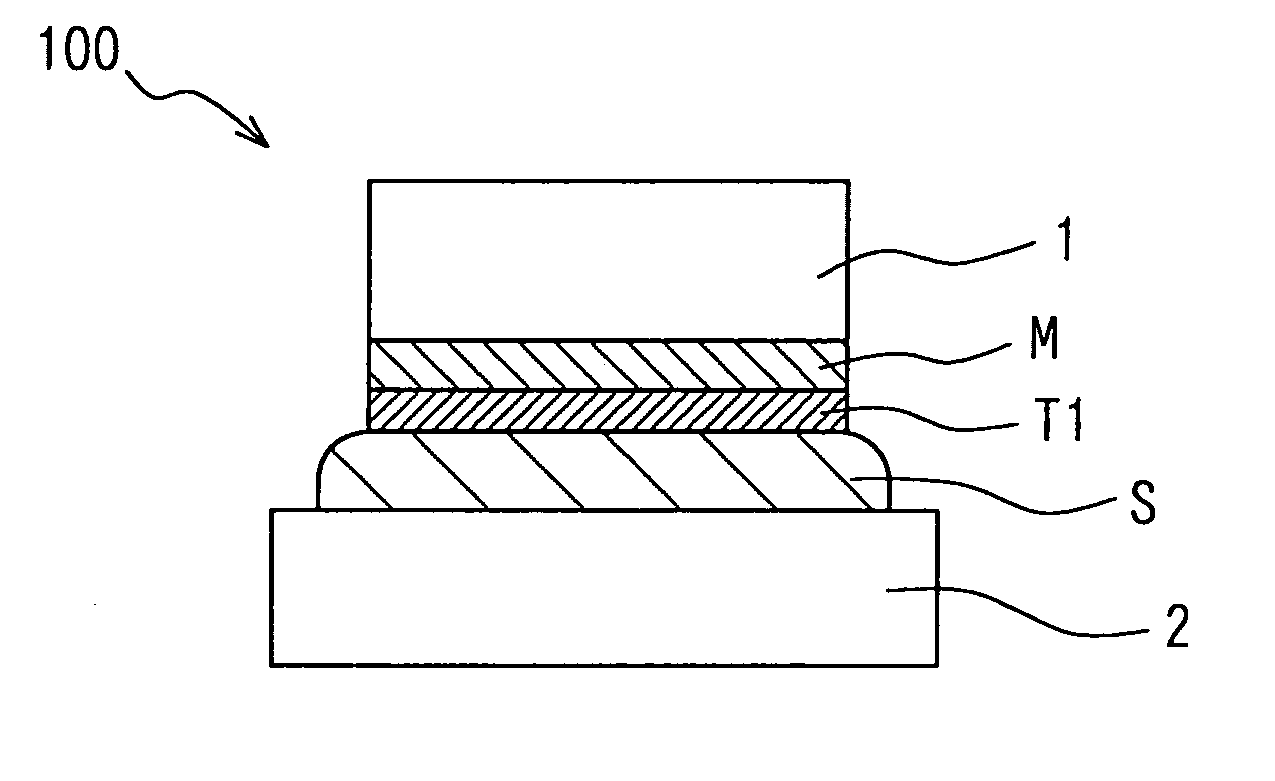
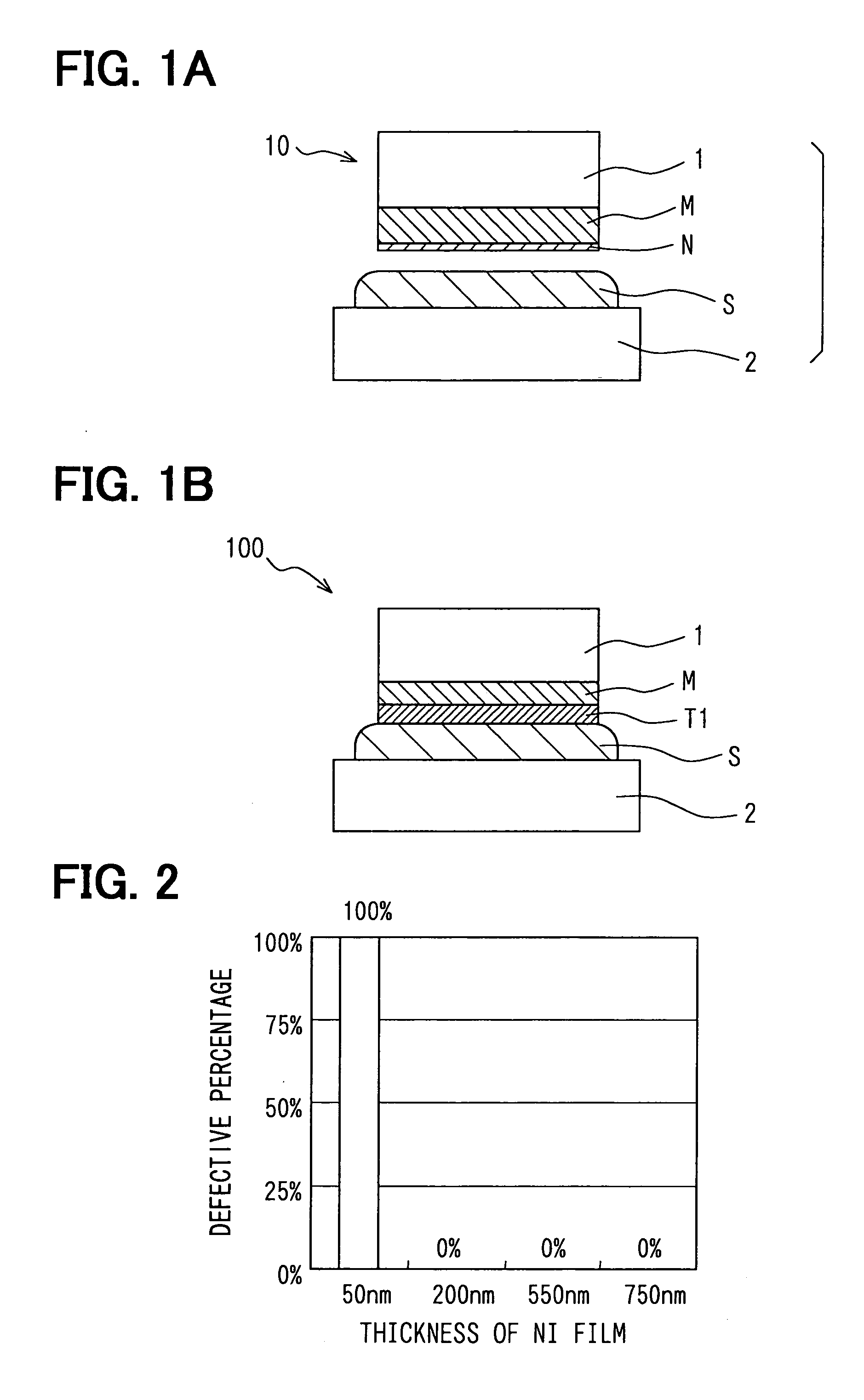
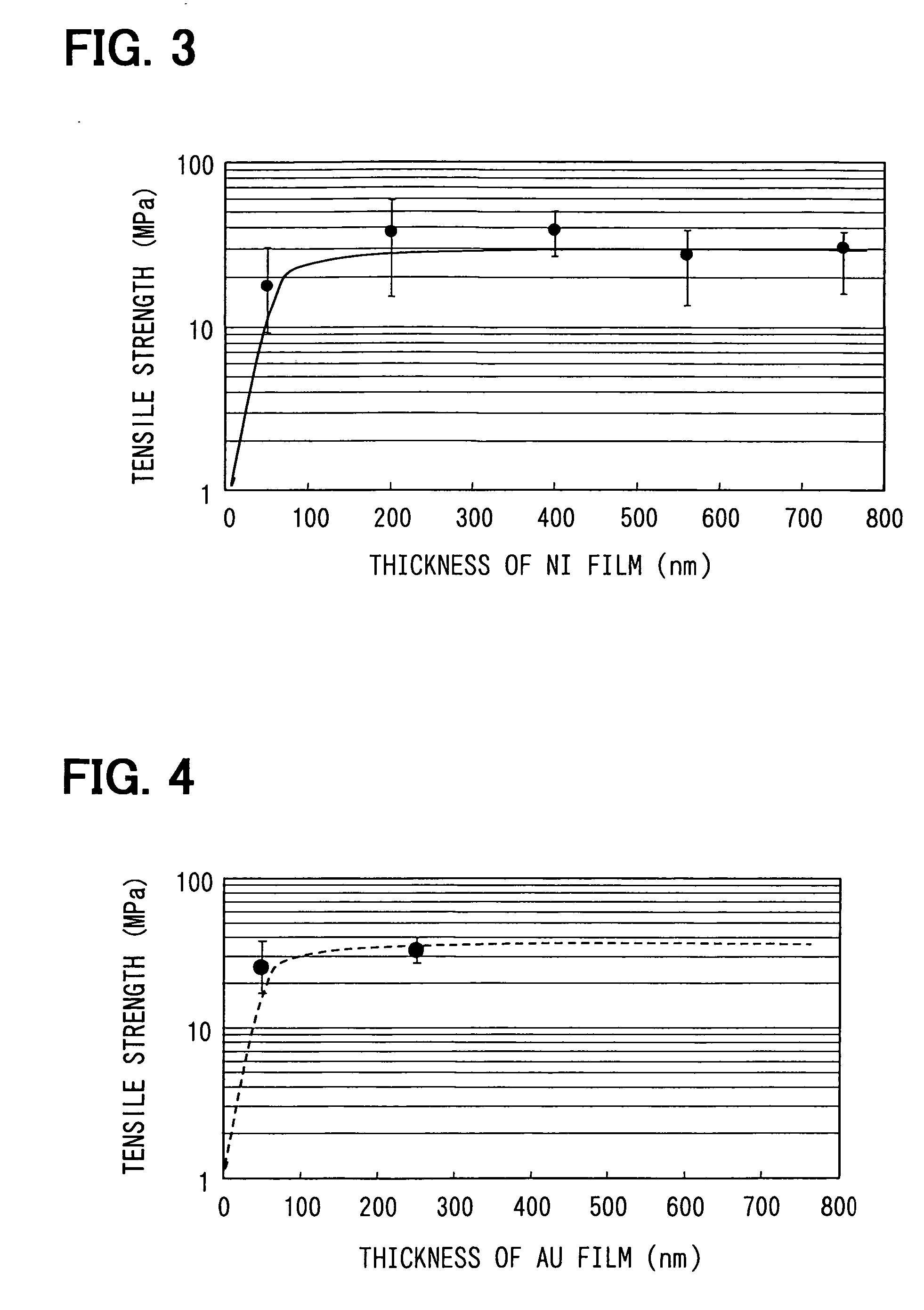
[0025] A semiconductor device 100 according to a first embodiment of the present invention is shown in FIGS. 1A and 1B. FIG. 1A shows the device 100 before heat treatment, i.e., before soldering, and FIG. 1B shows the device 100 after heat treatment, i.e., after soldering.

[0026] The device 100 includes a semiconductor substrate 1 and a base member 2. The substrate 1 has an electric part such as a power transistor formed on a foreside of the substrate 1. The backside of the substrate 1, which is opposite to the semiconductor part, is bonded on the base member 2 with a tin-based solder layer S. The base member 2 is, for example, a heat sink, a lead frame or a circuit board. The device 100 is manufactured as follows.

[0027] Firstly, the electric part is formed on the foreside of the substrate 1. The first metal layer M and the second metal layer N are formed on the backside of the substrate 1 in this order. Thus, a semiconductor chip 10 is formed. Then, the chip 10 is mounted on the b...

second embodiment

[0043] A semiconductor device 101 according to a second embodiment of the present invention is shown in FIGS. 6A to 6C. FIG. 6A shows the chip 10 before the first heat treatment, and FIG. 6B shows the chip 10 after the first heat treatment and the base member 2 before soldering. FIG. 6C shows the device 101 after the second heat treatment, i.e., after the soldering.

[0044] The device 101 is manufactured as follows. Firstly, the first metal layer M and the second metal layer N are formed on the backside of the substrate 1 in this order so that the semiconductor chip 10 is prepared. The chip 10 is firstly heated so that an intermediate alloy layer O is formed. The intermediate alloy layer O is composed of the first metal and the second metal alloy. The intermediate alloy layer O is disposed between the first and the second metal layers M, N. After this first heat treatment, the chip 10 is mounted on the base member 2 through the solder layer S. Then, the chip 10 with the base member 2...


PUM


Abstract

A semiconductor device includes: a semiconductor substrate; a base member; a tin-based solder layer; a first metal layer; and a first alloy layer. The semiconductor substrate is bonded to the base member through the first metal layer, the first alloy layer and the tin-based solder layer in this order. The first alloy layer is made of a first metal in the first metal layer and tin in the tin-based solder layer. The first metal layer is made of at least one of material selected from the group consisting of titanium, aluminum, iron, molybdenum, chromium, vanadium and iron-nickel-chromium alloy.

Description

CROSS REFERENCE TO RELATED APPLICATIONS [0001] This application is based on Japanese Patent Applications No. 2004-261425 filed on Sep. 8, 2004, and No. 2004-368114 filed on Dec. 20, 2004, the disclosures of which are incorporated herein by reference. FIELD OF THE INVENTION [0002] The present invention relates to a semiconductor device having a tin-based solder layer and a method for manufacturing the same. BACKGROUND OF THE INVENTION [0003] Conventionally, lead-tin alloy (Pb—Sn alloy) solder is used for bonding a semiconductor substrate such as an IC chip having a semiconductor device to a base member such as a heat sink and a lead frame. However, in view of environmental protection such as safety and low harmfulness, it is required to use Pb free solder or low Pb contained solder. One of Pb free solders is a tin-based solder. [0004] Japanese Patent Application Publication No. 2003-347487 discloses that a backside of a semiconductor substrate is bonded to a base member with a tin-ba...

Claims


Application Information

Patent Timeline
IPC IPC(8): H01L23/48
CPCH01L24/29H01L2924/157H01L24/83H01L2224/04026H01L2224/29111H01L2224/83801H01L2924/01005H01L2924/01013H01L2924/01015H01L2924/01029H01L2924/0103H01L2924/01032H01L2924/01042H01L2924/01046H01L2924/01047H01L2924/01049H01L2924/0105H01L2924/01051H01L2924/01078H01L2924/01079H01L2924/01082H01L2924/14H01L2224/83193H01L2924/01006H01L2924/01023H01L2924/01024H01L2924/01033H01L2924/014H01L2224/29101H01L2924/0132H01L2224/8482H01L2224/29109H01L2924/0133H01L2224/32245H01L24/32H01L2924/00H01L2924/01014H01L2924/01022H01L2924/01028H01L2924/01026H01L2924/00012H01L2924/00014H01L23/4827H01L2224/37099
Inventor KAYUKAWA, KIMIHARUTANAHASHI, AKIRANORITAKE, CHIKAGEMIURA, SHOJI
Owner DENSO CORP
Why Eureka
Try Eureka