Organic light emitting display and method of fabricating the same

a light-emitting display and organic technology, applied in the direction of discharge tube luminescnet display, discharge tube/lamp details, organic semiconductor devices, etc., can solve the problems of pixel electrode damage, less fabrication process, and drop in yield, so as to improve the effect of organic light-emitting display

Inactive Publication Date: 2006-03-09
SAMSUNG DISPLAY CO LTD
View PDF1 Cites 19 Cited by
  • Summary
  • Abstract
  • Description
  • Claims
  • Application Information

AI Technical Summary

Benefits of technology

[0009] It is therefore an object of the present inventio

Problems solved by technology

Thus, a material having a greater electromotive force corrodes due to galvanic corrosion, thereby damaging the pixel electrode.
However, in this case, the number of photoli

Method used


Image

  • Organic light emitting display and method of fabricating the same
  • Organic light emitting display and method of fabricating the same
  • Organic light emitting display and method of fabricating the same

Examples


Embodiment Construction

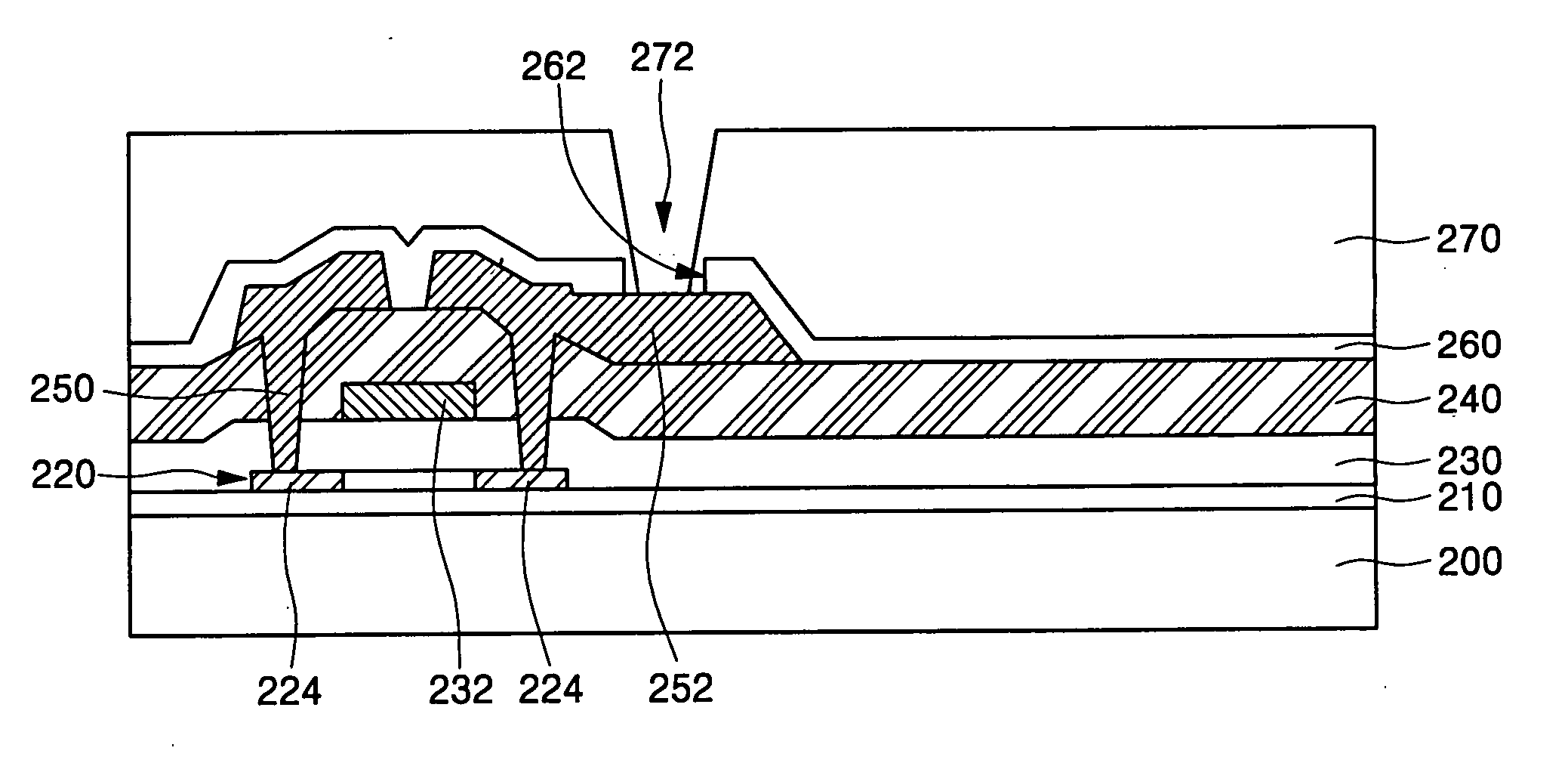
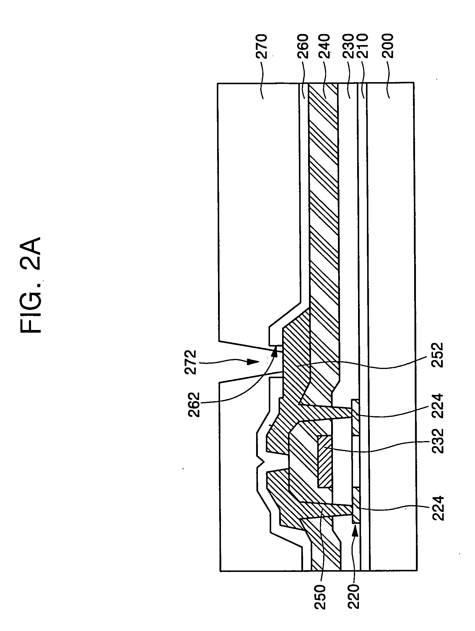
[0023] Hereinafter, a conventional structure of an organic light emitting display and preferable embodiments according to the present invention will be described with reference to the accompanying drawings. Here, when one element is connected to another element, one element may be not only directly connected to another element but also indirectly connected to another element via another element. Further, irrelative elements are omitted for clarity. Also, like reference numerals refer to like elements throughout.

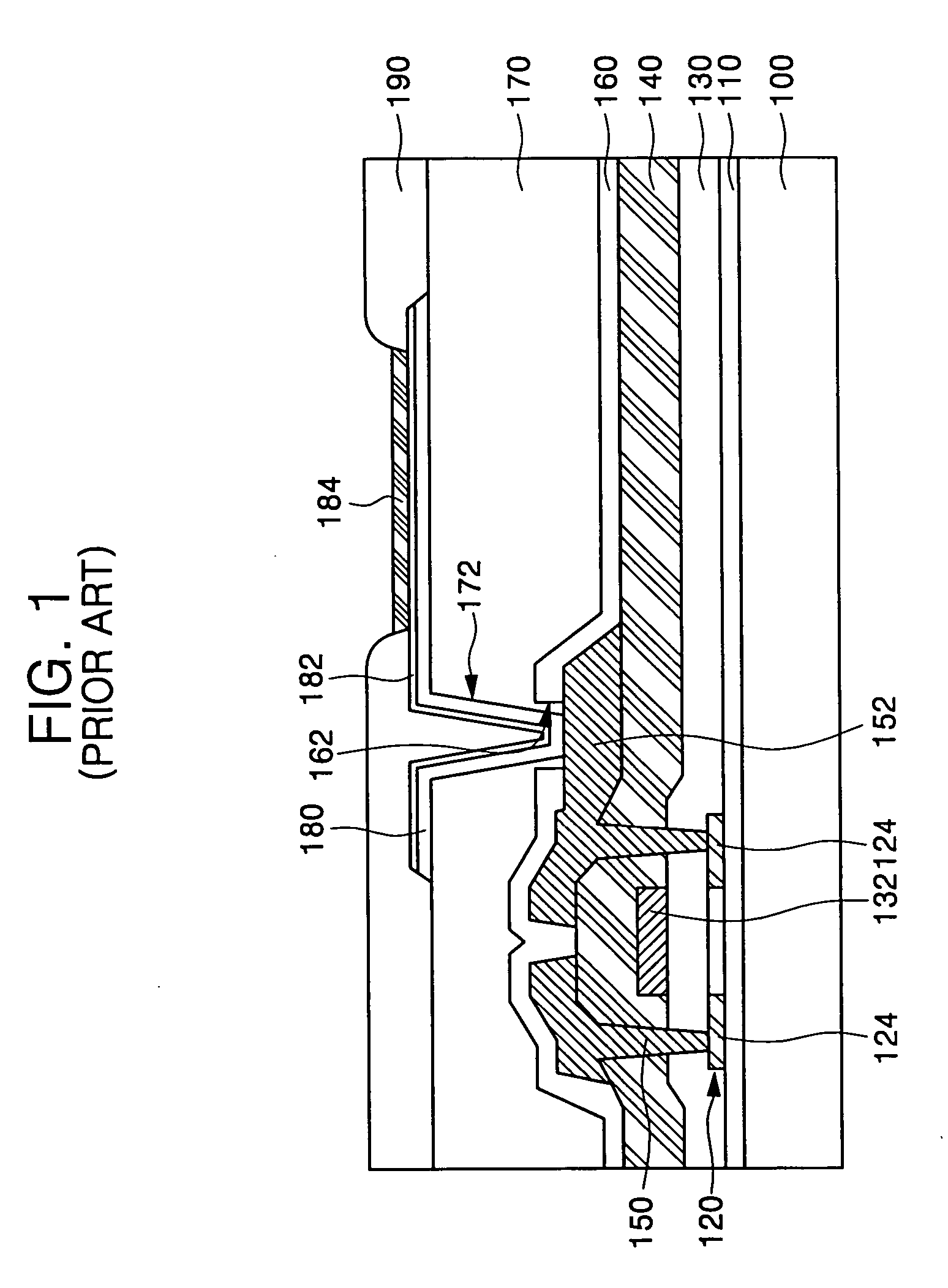
[0024]FIG. 1 is a schematic cross-sectional view of a conventional organic light emitting display.

[0025] Referring to FIG. 1, a buffer layer 110 having a predetermined thickness is formed on a substrate 100, and a thin-film transistor (TFT) including a polycrystalline silicon (poly-Si) pattern 120, a gate electrode 132, a source electrode 150, and a drain electrode 152 is formed. In this case, source and drain regions 124, which are ion-implanted with impurities, are dispos...


PUM


Abstract

An OLED and a method of fabricating the same are provided, in which, when a reflective layer pattern is formed, a thin layer for a pixel electrode is opened at an edge of an emission region to form the pixel electrode without additional photolithography and etching processes by forming an undercut under the edge of the reflective layer pattern, i.e., under the edge of the emission region by over-etching, thereby simplifying the process and increasing the yield.

Description

CLAIM OF PRIORITY [0001] This application claims priority to and the benefit of Korean Patent Application No. 2004-71891, filed Sep. 8, 2004, which is hereby incorporated by reference for all purposes as if fully set forth herein. BACKGROUND OF THE INVENTION [0002] 1. Field of the Invention [0003] The present invention relates to an organic light emitting display (OLED) and method of fabricating the same and, more particularly, to an OLED and method of fabricating the same, which can simplify the fabricating process by automatically patterning a pixel electrode. [0004] 2. Discussion of the Background [0005] In general, an OLED is a self-emissive display in which light is emitted by exciting fluorescent organic compounds. The OLED can be classified into a passive matrix OLED (PMOLED) and an active matrix OLED (AMOLED) according to a driving method of N×M pixels, which are arranged in a matrix shape. In comparison with the PMOLED, the AMOLED is suitable for large-area displays due to ...

Claims


Application Information

Patent Timeline
IPC IPC(8): H05B33/00
CPCH01L27/3244H01L2251/5315H01L51/56H01L51/5206H10K59/124H10K59/12H10K50/818H10K2102/3026H10K71/00H05B33/22H05B33/10
Inventor KANG, TAE-WOOKLEE, KWAN-HEE
Owner SAMSUNG DISPLAY CO LTD
Why Eureka
Try Eureka