

Non-volatile semiconductor memory device
a non-volatile, semiconductor technology, applied in the direction of static storage, digital storage, instruments, etc., can solve the problem of failure of write sequen
- Summary
- Abstract
- Description
- Claims
- Application Information
AI Technical Summary
Benefits of technology
Problems solved by technology
Method used
Image

Examples
embodiment 1
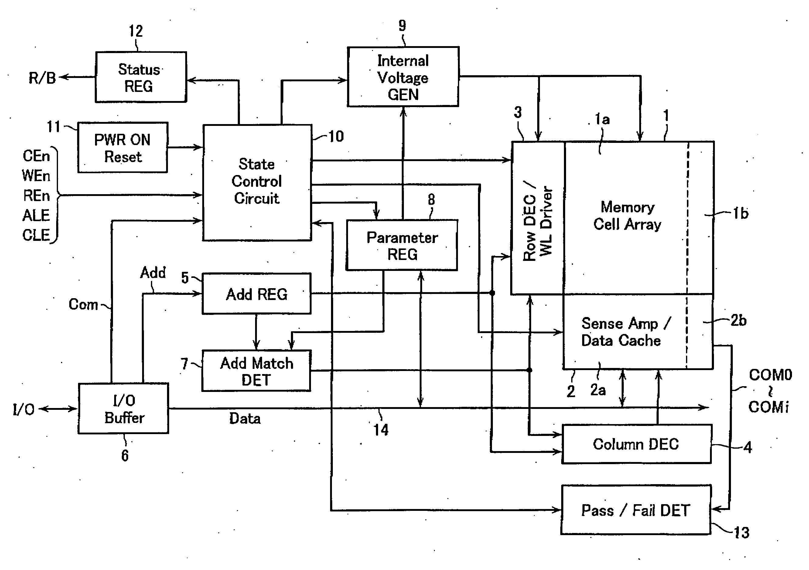
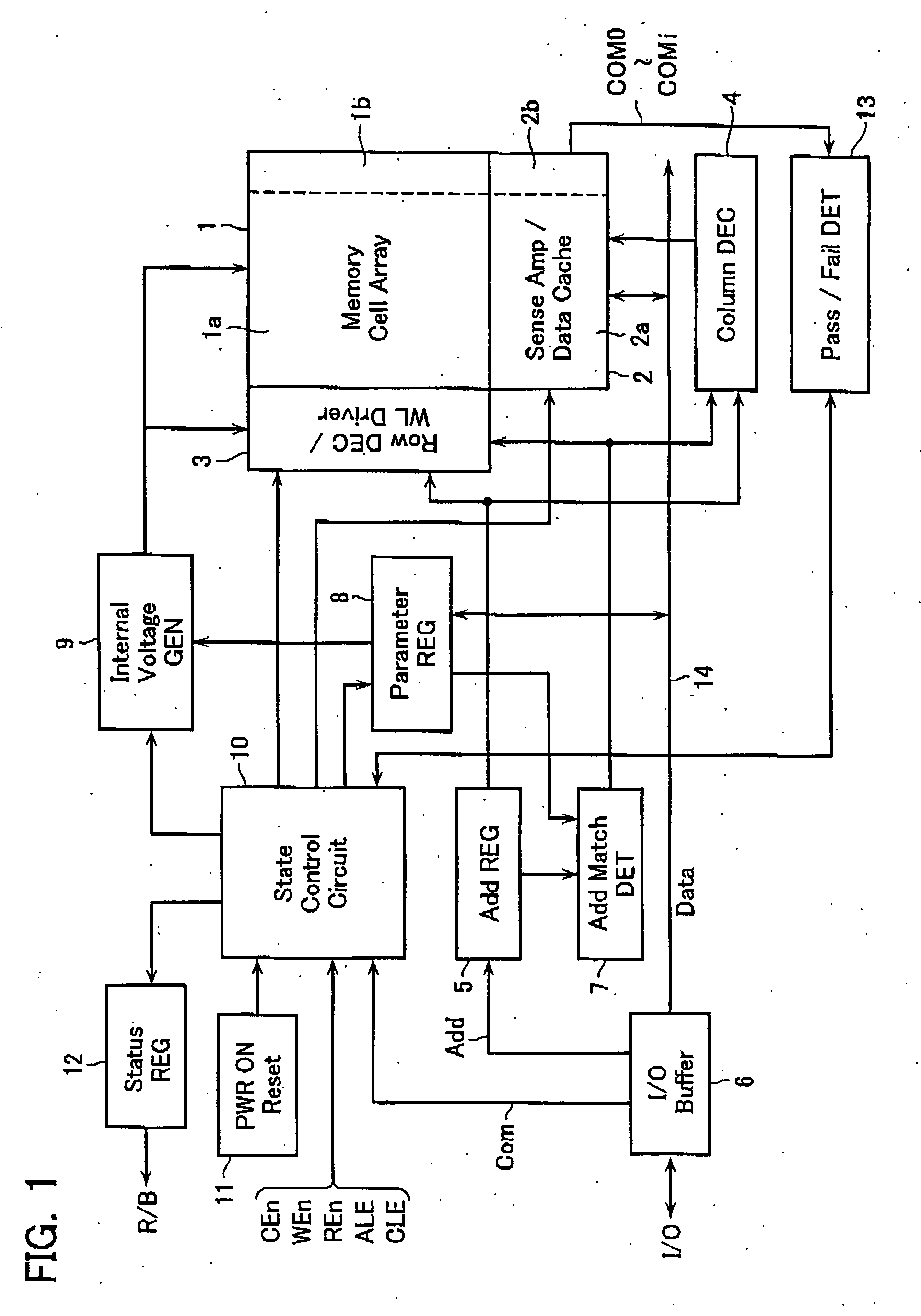
[0042]FIG. 1 shows a functional block configuration of a flash memory in accordance with an embodiment, and FIG. 2 shows an arrangement of the memory cell array 1.
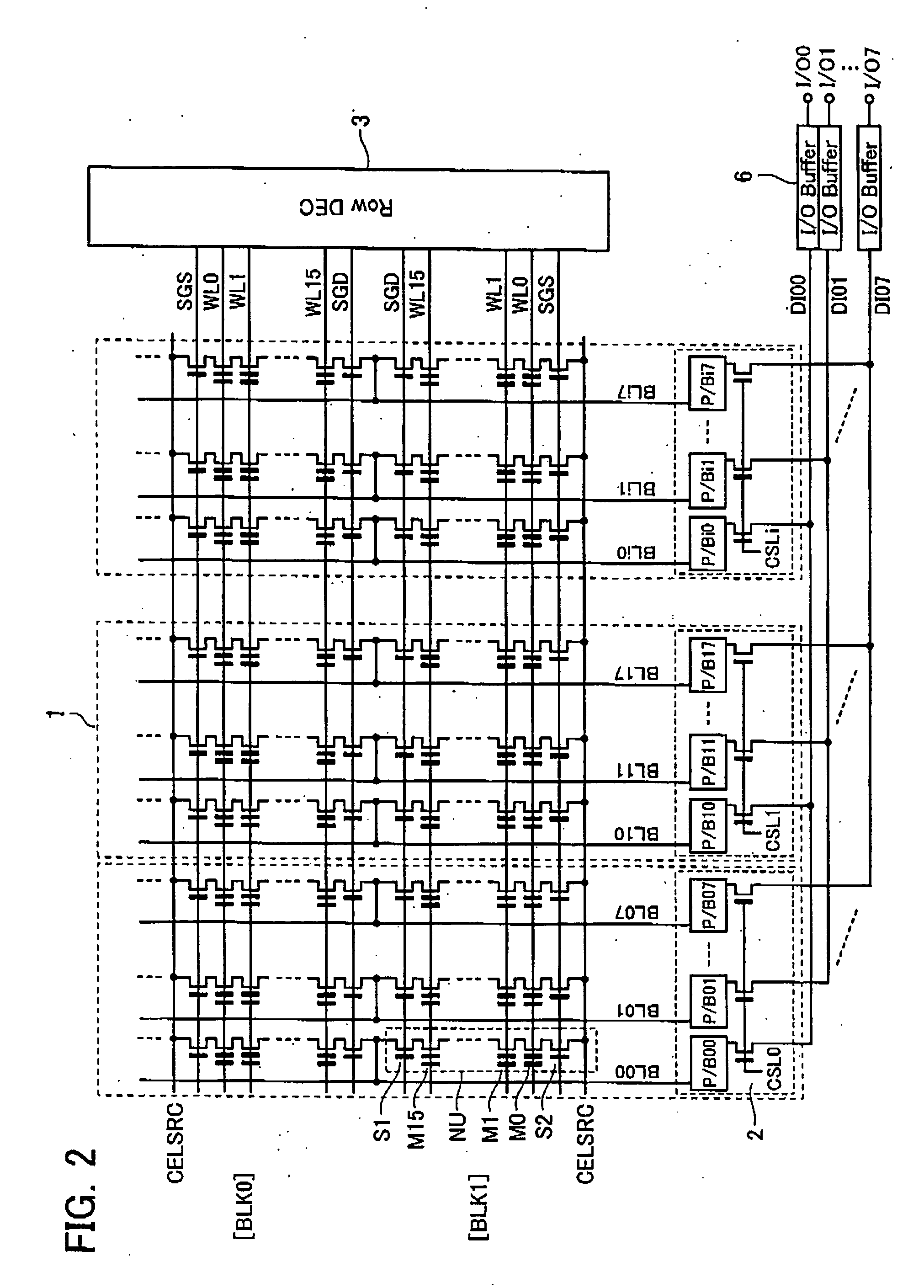
[0043] The memory cell array 1 is formed of NAND cell units NU arranged in a matrix manner. Each NAND cell unit NU has a plurality of (sixteen in the example shown in FIG. 2) memory cells M0-M15 connected in series and select gate transistors S1 and S2 disposed at both ends thereof. The select gate transistors S1 and S2 couple the both ends of the memory cell string to a bit line BL and a source line CELSRC, respectively.
[0044] Control gates of the memory cells in a NAND cell unit are coupled to different word lines WL0-WL15. Gates of the select gate transistors S1 and S2 are coupled to select gate lines SGD and SGS, respectively.
[0045] A set of NAND cell units sharing word lines WL0-WL15 constitutes a block, which serves as a unit of data erase. As shown in FIG. 2, a plurality of blocks (BLK0, BLK1, . . . ) are arrange...
embodiment 2
[0102] There will be provided another method of effectively shorten the write time without writing isolation data for defective columns found lately. FIG. 14 shows a write sequence using the above-described method.
[0103] Input a certain command, and this write sequence starts. Following the command, an address is input (step S11), and write data are loaded (step QS12). So far, it is the same as the above-described embodiment, and write operations are automatically executed hereinafter under the control of the controller 10.
[0104] In this embodiment, verify-judgment (pass / fail judgment) is executed in the background of the write step S13 based on the last verify-read data. Explaining in detail, in order to apply a write voltage, it is in need of taking a time for charging up write-inhibiting bit lines and non-selected bit lines. In this embodiment, the pass / fail judgment is executed within a preparation period necessary for applying the write voltage. If it is judged “Pass”, the da...
embodiment 3
[0113] As an embodiment, an electric card using the non-volatile semiconductor memory devices according to the above-described embodiments of the present invention and an electric device using the card will be described bellow.
[0114]FIG. 15 shows an electric card according to this embodiment and an arrangement of an electric device using this card. This electric device is a digital still camera 101 as an example of portable electric devices. The electric card is a memory card 61 used as a recording medium of the digital still camera 101. The memory card 61 incorporates an IC package PK1 in which the non-volatile semiconductor memory device or the memory system according to the above-described embodiments is integrated or encapsulated.
[0115] The case of the digital still camera 101 accommodates a card slot 102 and a circuit board (not shown) connected to this card slot 102. The memory card 61 is detachably inserted in the card slot 102 of the digital still camera 101. When inserted...
PUM
 Abstract
Description
Claims
Application Information