

NAND flash memory device and copyback program method for same
a flash memory and program method technology, applied in error detection/correction, digital storage, instruments, etc., can solve the problems of two-bit errors after copyback operation, additional one-bit errors may occur, etc., to prevent two-bit errors in one page
- Summary
- Abstract
- Description
- Claims
- Application Information
AI Technical Summary
Benefits of technology
Problems solved by technology
Method used
Image

Examples
Embodiment Construction
[0015] Specific embodiments of the invention will be described below in more detail with reference to the accompanying drawings. The invention may, however, be embodied in many different forms and should not be construed as limited only to the specific embodiments set forth below. Rather, these embodiments are provided so that this disclosure will be thorough and complete, and will fully convey the scope of the invention to those skilled in the art. In the specification, like numerals refer to like elements throughout.
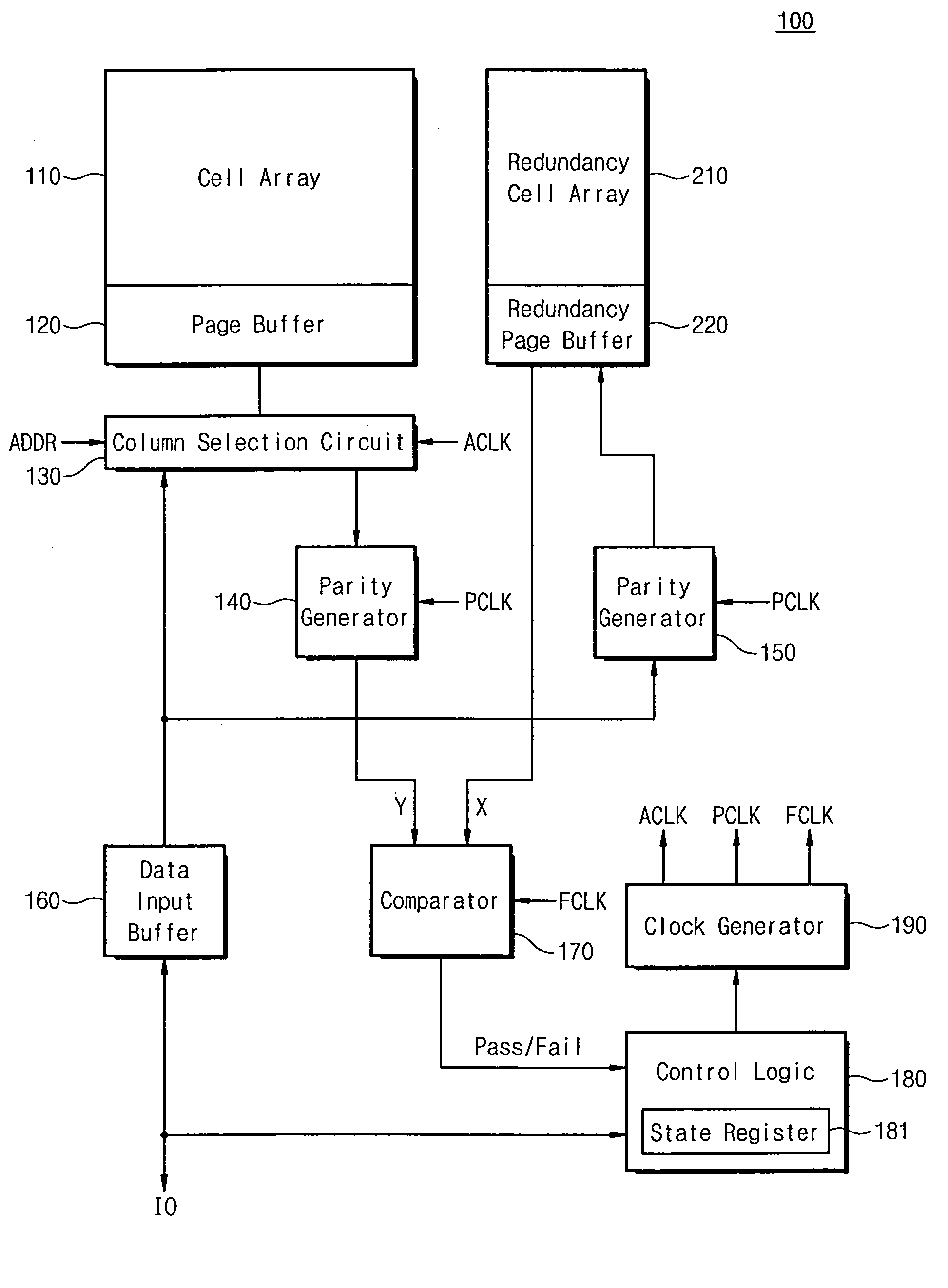
[0016]FIG. 1 is a block diagram illustrating a NAND flash memory device in accordance with some embodiments of the invention. Referring to FIG. 1, the NAND flash memory device 100 includes a cell array 110, a page buffer 120, a column selection circuit 130, parity generators 140 and 150, a data input buffer 160, a comparator 170, a control logic 180, a clock generator 190, a redundancy cell array 210, and a redundancy page buffer 220.
[0017] The data input buffer 160 ...
PUM
 Abstract
Description
Claims
Application Information