System and method detecting malfunction of pad conditioner in polishing apparatus

a polishing apparatus and pad conditioner technology, applied in the field of polishing apparatuses, can solve the problems of difficult to obtain a truly flat surface (e.g., an accurate topology) using only chemical polishing, and the typical sequence of processes used in the manufacture of semiconductor devices is long and complicated

Inactive Publication Date: 2006-03-09
SAMSUNG ELECTRONICS CO LTD
View PDF5 Cites 8 Cited by
  • Summary
  • Abstract
  • Description
  • Claims
  • Application Information

AI Technical Summary

Benefits of technology

[0014] Embodiments of the invention are directed a polishing apparatus and method of use in which malfunctions related to a conditioning pad are detected and associated degradation in polishing uniformity and wafer defects are avoided accordingly.

Problems solved by technology

The typical sequence of processes used to manufacture semiconductor devices is a long and complicated one.
However, it is often difficult to obtain a truly flat surface (e.g., an accurate topology) using only chemical polishing.
However, one notable exception to this excellent track record is reoccurring problems with a conditioning pad installed in opposition to the platen.
Such conditioning pads have a frequent rate of malfunction.
This frequent state of malfunction can cause larger problems, because if the conditioning pad is not regularly applied to the polishing pad (typically before and / or after each polishing process) problems arise, such as inadequate polishing rates and degraded polishing uniformity.
These results threaten the reliability of semiconductor devices formed on the wafer.

Method used


Image

  • System and method detecting malfunction of pad conditioner in polishing apparatus
  • System and method detecting malfunction of pad conditioner in polishing apparatus
  • System and method detecting malfunction of pad conditioner in polishing apparatus

Examples


Embodiment Construction

)

[0029] The present invention will now be described in some additional detail with reference to one or more embodiments(s) shown in the accompanying drawings.

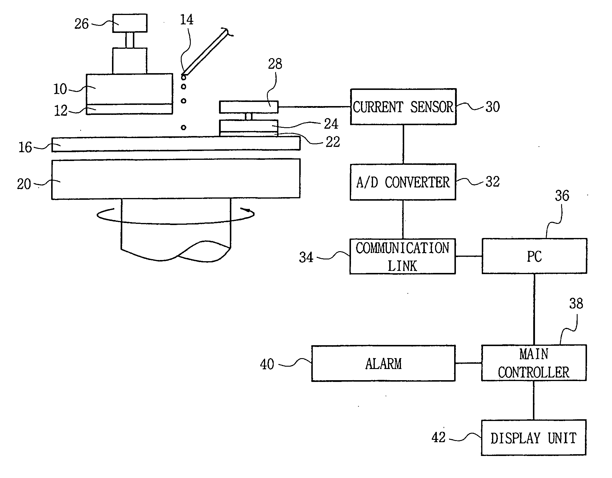
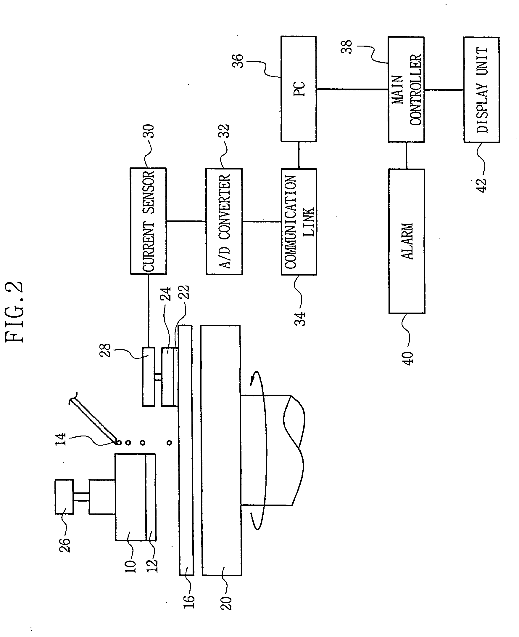
[0030]FIG. 2 is a system diagram of a polishing apparatus for semiconductor wafer according to the present invention.

[0031] The polishing apparatus generally comprises: a polishing pad 16 for polishing a wafer 12; a platen 20 for fixing (e.g., seating) and rotating polishing pad 16; and a polishing head 10 installed in counterpoise to polishing pad 16. Wafer 12 is seated on polishing head 10 by means of vacuum. The polishing apparatus also comprises a motor 26 adapted to rotate polishing head 10.

[0032] Additionally, the polishing apparatus comprises a pad conditioner comprising a conditioning pad 22 adapted to condition polishing pad 16 and seated on a conditioner head 24. Conditioning pad 22 is also provide in counterpoise to polishing pad 16. A drive motor 28 is coupled to conditioner head 24 and is adapted to rotate condi...


PUM

PropertyMeasurementUnit
characteristic voltageaaaaaaaaaa
currentaaaaaaaaaa

Abstract

A system and method adapted to detect a malfunction related to a pad conditioner in a polishing apparatus are disclosed. The pad conditioner includes a conditioning pad seated on a conditioner head and a drive motor rotating the conditioner head. The system also comprises a current sensor connected to the drive motor, adapted to detect electrical current drawn by the drive motor, and provide a corresponding current value, a Personal Computer (PC) receiving the current value, adapted to compare the received current value to first and second reference values, and generate a drive indication signal in response to the comparison, and a main controller receiving the drive indication signal and adapted to generate an interlock signal halting operation of the polishing apparatus in response to the drive indication signal.

Description

BACKGROUND OF THE INVENTION [0001] 1. Technical Field [0002] The present invention generally relates to a polishing apparatus (or system) useful in the fabrication and processing of semiconductor wafers. More particularly, the invention relates to a device and related method adapted to detect a malfunction related to a pad conditioner in the polishing apparatus. [0003] This application claims the benefit of Korean Patent Application No. 10-2004-0071967, filed Sep. 9, 2004, the disclosure of which is hereby incorporated by reference in its entirety. [0004] 2. Discussion of Related Art [0005] The typical sequence of processes used to manufacture semiconductor devices is a long and complicated one. Many individual semiconductor devices are manufactured on a single substrate. This substrate is usually provided in the form of a thin wafer of semiconductor material. [0006] Over time, semiconductor devices have been formed a wafer with ever increasing height profiles. Increased height prof...

Claims


Application Information

Patent Timeline
Patent Type & Authority Applications(United States)
IPC IPC(8): B24B51/00B24B1/00
CPCB24B53/017B24B49/16H01L21/302H01L21/304
Inventor KIM, HYEUNG-YEULKIM, SUNG-HWAN
Owner SAMSUNG ELECTRONICS CO LTD
Why Eureka
Try Eureka