Compact SCR device and method for integrated circuits

Inactive Publication Date: 2006-03-16
ALTERA CORP
View PDF20 Cites 7 Cited by
  • Summary
  • Abstract
  • Description
  • Claims
  • Application Information

AI Technical Summary

Benefits of technology

[0011] Many benefits are achieved by way of the present invention over conventional techniques. For example, certain embodiments of the present invention provide a single device allowing ESD discharge in both polarity. For example, the single device includes both PNPN SCR and NPNP SCR, and PNPN SCR and NPNP SCR share diffusion areas. Some embodiments of the present invention provide fast turn-on of the device for effective ESD protection. Certain embodiments of the present invention provid

Problems solved by technology

The integrated circuits may be damaged by the discharge of electrostatic energy.
But the diodes can significantly increase junction capac

Method used


Image

  • Compact SCR device and method for integrated circuits
  • Compact SCR device and method for integrated circuits
  • Compact SCR device and method for integrated circuits

Examples


Embodiment Construction

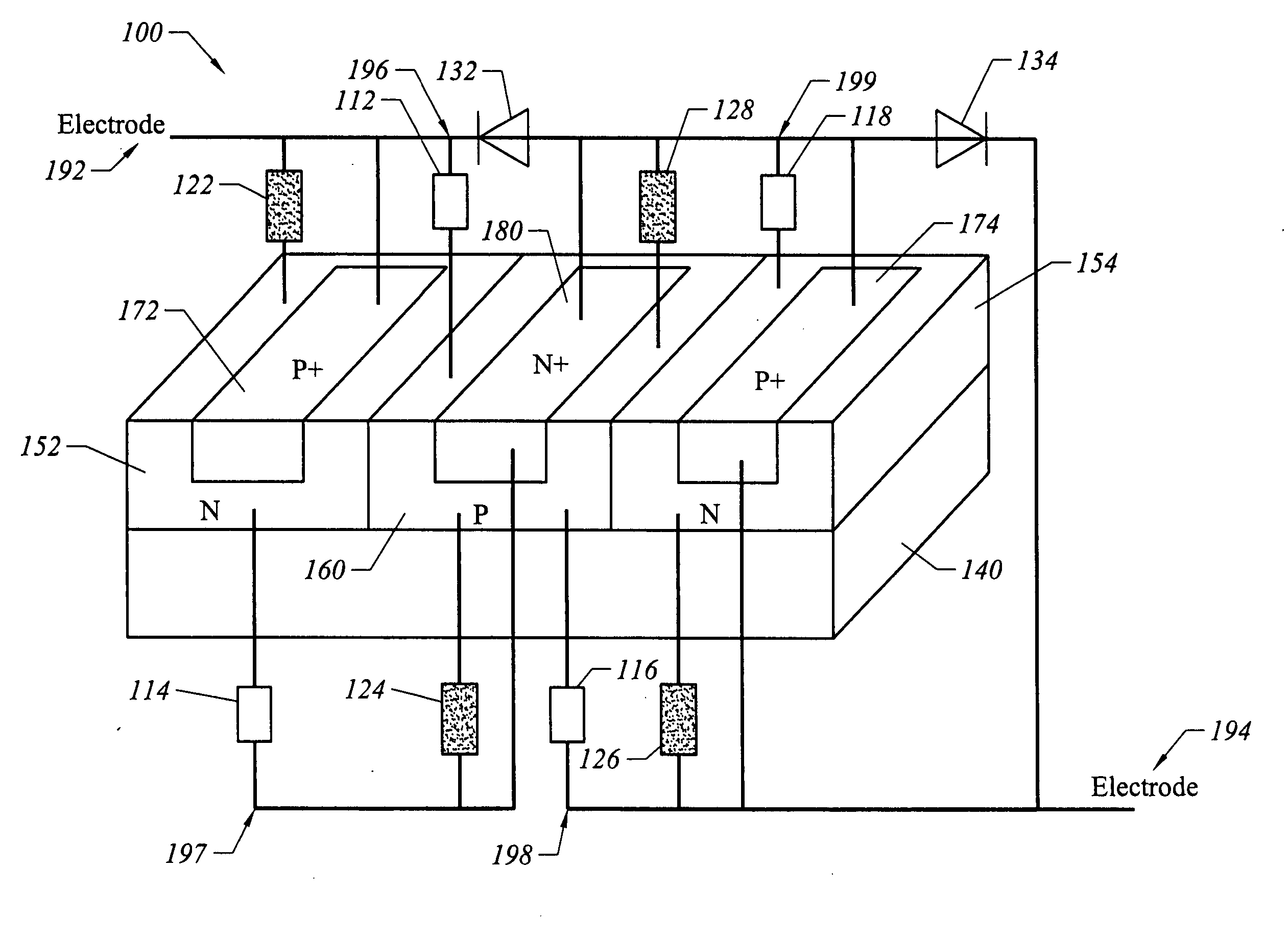
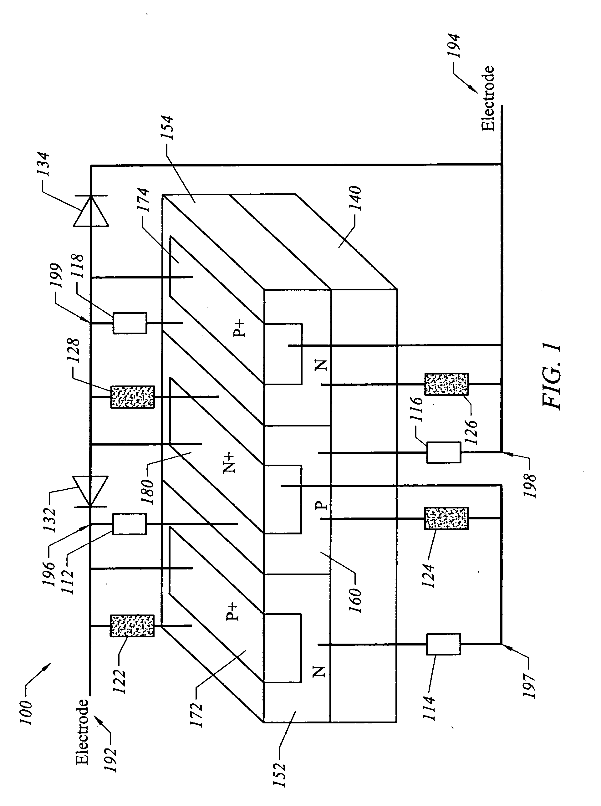
[0030] The present invention relates generally to electrostatic discharge (ESD) protection. More specifically, the invention provides a compact semiconductor controlled rectifier (SCR) device and method. Merely by way of example, the invention has been applied to integrated circuits with silicon on insulator (SOI), but it would be recognized that the invention has a much broader range of applicability.

[0031]FIG. 1 is a simplified diagram for a compact SCR device according to an embodiment of the present invention. This diagram is merely an example, which should not unduly limit the scope of the claims herein. The device 100 includes triggering devices 112, 114, 116, and 118, resistors 122, 124, 126, and 128, diodes 132 and 134, insulating layer 140, n regions 152 and 154, p region 160, p+ regions 172 and 174, n+ region 180, and electrodes 192 and 194. Although the above has been shown using a selected group of components, there can be many alternatives, modifications, and variation...


PUM


Abstract

A semiconductor device and method for electrostatic discharge protection. The semiconductor device includes a first semiconductor controlled rectifier and a second semiconductor controlled rectifier. The first semiconductor controlled rectifier includes a first semiconductor region and a second semiconductor region, and the second semiconductor controlled rectifier includes the first semiconductor region and the second semiconductor region. The first semiconductor region is associated with a first doping type, and the second semiconductor region is associated with a second doping type different from the first doping type. The second semiconductor region is located directly on an insulating layer.

Description

CROSS-REFERENCES TO RELATED APPLICATIONS [0001] Not Applicable STATEMENT AS TO RIGHTS TO INVENTIONS MADE UNDER FEDERALLY SPONSORED RESEARCH OR DEVELOPMENT [0002] Not Applicable REFERENCE TO A “SEQUENCE LISTING,” A TABLE, OR A COMPUTER PROGRAM LISTING APPENDIX SUBMITTED ON A COMPACT DISK. [0003] Not Applicable BACKGROUND OF THE INVENTION [0004] The present invention relates generally to electrostatic discharge (ESD) protection. More specifically, the invention provides a compact semiconductor controlled rectifier (SCR) device and method. Merely by way of example, the invention has been applied to integrated circuits with silicon on insulator (SOI), but it would be recognized that the invention has a much broader range of applicability. [0005] The integrated circuits may be damaged by the discharge of electrostatic energy. The damage may be prevented by protection devices or circuits which shunt the ESD energy away from the integrated circuits. The protection devices include at least ...

Claims


Application Information

Patent Timeline
IPC IPC(8): H01L23/62
CPCH01L29/74H01L27/0262
Inventor O, HUGH SUNGKISHIH, CHIH-CHINGHUANG, CHENG-HSIUNG
Owner ALTERA CORP
Why Eureka
Try Eureka