A low-trigger negative-voltage-resistant SCR device, process method, and application circuit

A technology for triggering circuits and process methods, which is applied in circuits, electric solid-state devices, semiconductor devices, etc., and can solve the problems of high trigger voltage and inability to achieve ESD protection.

Active Publication Date: 2017-09-19
SHENZHEN STATE MICROELECTRONICS CO LTD
View PDF6 Cites 0 Cited by
  • Summary
  • Abstract
  • Description
  • Claims
  • Application Information

AI Technical Summary

Problems solved by technology

[0010] The purpose of the embodiment of the present invention is to provide an SCR device with negative voltage resistance and low trigger voltage, aiming to solve the problem that the trigger voltage of the existing SCR device is higher than the breakdown voltage of the internal gate oxide layer of the chip, and cannot achieve effective ESD protection.

Method used


Image

  • A low-trigger negative-voltage-resistant SCR device, process method, and application circuit
  • A low-trigger negative-voltage-resistant SCR device, process method, and application circuit
  • A low-trigger negative-voltage-resistant SCR device, process method, and application circuit

Examples


Embodiment Construction

[0040] In order to make the object, technical solution and advantages of the present invention clearer, the present invention will be further described in detail below in conjunction with the accompanying drawings and embodiments. It should be understood that the specific embodiments described here are only used to explain the present invention, not to limit the present invention. In addition, the technical features involved in the various embodiments of the present invention described below can be combined with each other as long as they do not constitute a conflict with each other.

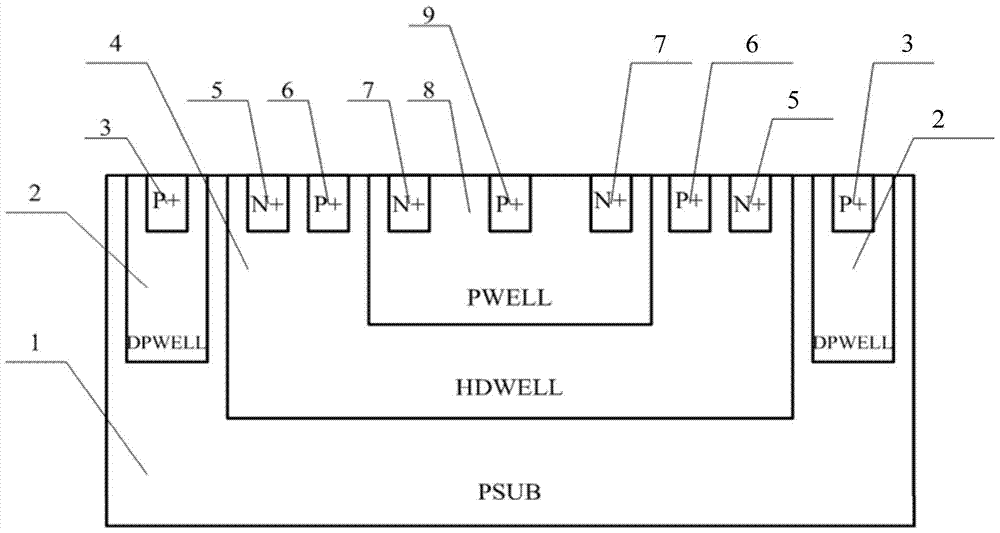
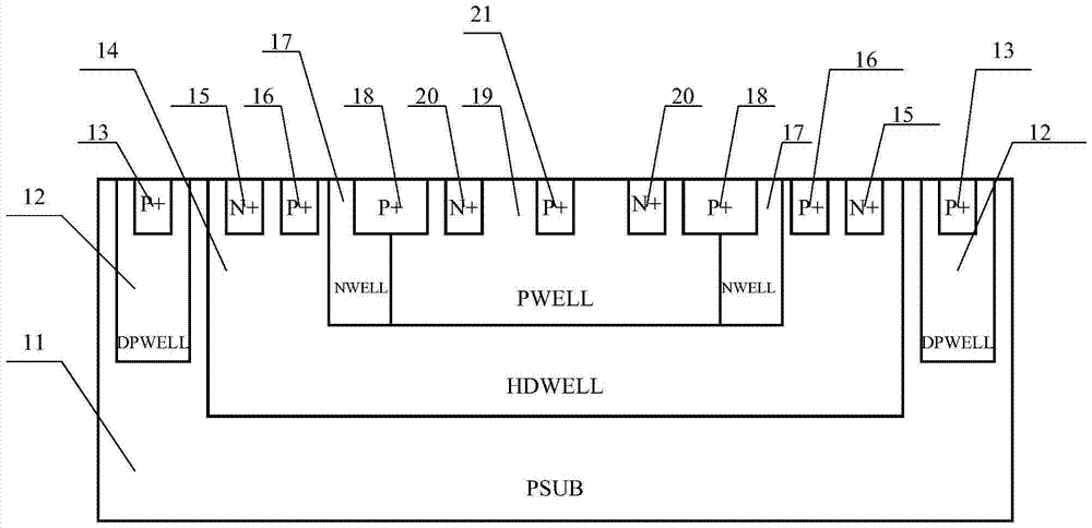
[0041] The negative-voltage-resistant SCR device with low trigger voltage provided by the embodiment of the present invention can effectively reduce the trigger voltage of the negative-voltage-resistant SCR device, so that the trigger voltage is lower than the breakdown voltage of the internal gate oxide layer of the chip, thereby achieving effective ESD Protection design requirements.

[0042]...


PUM


Abstract

The present invention is applicable to the field of semiconductor devices, and provides an SCR device with low trigger negative voltage resistance, a process method and an ESD application circuit. The device includes: a substrate, a first deep implant well formed in the substrate, and A first active region formed in a deep implant well; a second deep implant well formed in the substrate, a second active region formed in the second deep implant well, and a second deep implant well formed in the second deep implant well The first active region; the second well formed in the second deep implanted well, the first well formed in the second deep implanted well, the first well formed by simultaneous implantation into the two wells at the junction of the first and second wells An active region, a second active region formed in the first well, and a first active region formed in the first well. The negative-voltage-resistant SCR device with low trigger voltage provided by the invention can reduce the trigger voltage of the negative-voltage-resistant SCR device to below the breakdown voltage of the internal gate oxide layer of the chip, thereby realizing the design requirement of effective ESD protection.

Description

technical field [0001] The invention belongs to the field of semiconductor devices, in particular to an SCR device with low trigger negative voltage resistance, a process method and an ESD application circuit. Background technique [0002] Compared with other electrostatic protection (ESD) devices, silicon controlled rectifier (SCR) devices have higher protection performance per unit area due to their low holding voltage characteristics. [0003] figure 1 Shows the cross-sectional structure of an existing high trigger negative voltage withstand SCR device, the SCR device structure includes: a P-type substrate (PSUB) 1, a plurality of deep implanted P wells formed in the P-type substrate 1 by doping (DPWELL) 2, and the P+ active region (P+) 3 formed by doping in each deep implanted P well 2, the P type substrate 1 is grounded through the P+ active region 3 through the deep implanted P well 2; [0004] The SCR device structure also includes: a deep implanted N well (HDWELL) ...

Claims


Application Information

Patent Timeline
Patent Type & Authority Patents(China)
IPC IPC(8): H01L27/02H01L29/74H01L21/332
Inventor 杜明裴国旭刘玲陈瑞军汤波
Owner SHENZHEN STATE MICROELECTRONICS CO LTD
Why Eureka
Try Eureka