Analogue switch

a technology of analog switch and offset voltage, applied in the field of analog switch, can solve the problems of increasing circuit cost, and achieve the effect of reducing the offset voltage across the switch and operating efficiently

Inactive Publication Date: 2006-03-30
ZETEK
View PDF8 Cites 10 Cited by
  • Summary
  • Abstract
  • Description
  • Claims
  • Application Information

AI Technical Summary

Benefits of technology

[0017] An advantage of the present invention is that the analogue switch allows for bi-directional current flow. The switch may operate efficiently with the voltage at the first switch terminal being higher than the voltage at the second switch terminal, or the other way round. As such, the load may be connected to either switch terminal. Additionally, the offset voltage across the switch is significantly reduced compared with the offset voltage for an analogue switch in accordance with the prior art.
[0018] The switching circuit may further comprise a first current source for supply of a first control current to the base of the first transistor. The switching circuit may further comprise a second current source for supply of a second control current to the base of the second transistor. Alternatively, the switching circuit may further comprise a common current source for supply of said control current to the base of each transistor. The common current source may be arranged to supply said control current to the base of each transistor either independently or together.
[0019] An advantage of the present invention is that the switch may be turned on by supplying current to either or both of the bases of the first and second transistors. If the voltage to be switched at the first switch terminal is higher than the voltage at the second switch terminal then the switch may most simply be turned on by supplying the first control current to the base of the first transistor. If the voltage to be switched at the first switch terminal is lower than the voltage at the second switch terminal then the switch may be most simply turned on by supply the second control current to the base of the second transistor. Alternatively, and most simply the control current may be supplied to the bases of both transistors. Supplying the control current to the bases of both transistors is advantageous as this removes the need to determine the relative voltage levels at the switch terminals before turning the switch on.
[0020] A further advantage of the present invention is that the control current to the first and second transistors may be supplied from separate current sources or a common current source. The common current source may supply the control current to both transistors at the same time, or independently.
[0021] Preferably, the first and second bipolar transistors are matched transistors.
[0022] Preferably, the switching circuit further comprises a slave switching circuit comprising first and second slave terminals, a slave switch, the slave switch comprising a third bipolar transistor, having a collector connected to the first slave terminal and an emitter connected to the second slave terminal, and a fourth bipolar transistor, having an emitter connected to the first slave terminal and a collector connected to the second slave terminal, a first controlled current source having a programming input connected to the first slave terminal and a current output connected to the first switch terminal and a second controlled current source having a programming input connected to the second slave terminal and a current output connected to the second switch terminal. The slave switch can be turned on by supply of a slave control current to the base of at least one of the third or the fourth bipolar transistor.

Problems solved by technology

This may be due to limitations imposed by the requirements of the circuit on the fabrication process.
Combining bipolar and MOSFET circuits in a single integrated circuit increases the expense of the circuit.

Method used


Image

  • Analogue switch
  • Analogue switch
  • Analogue switch

Examples


first embodiment

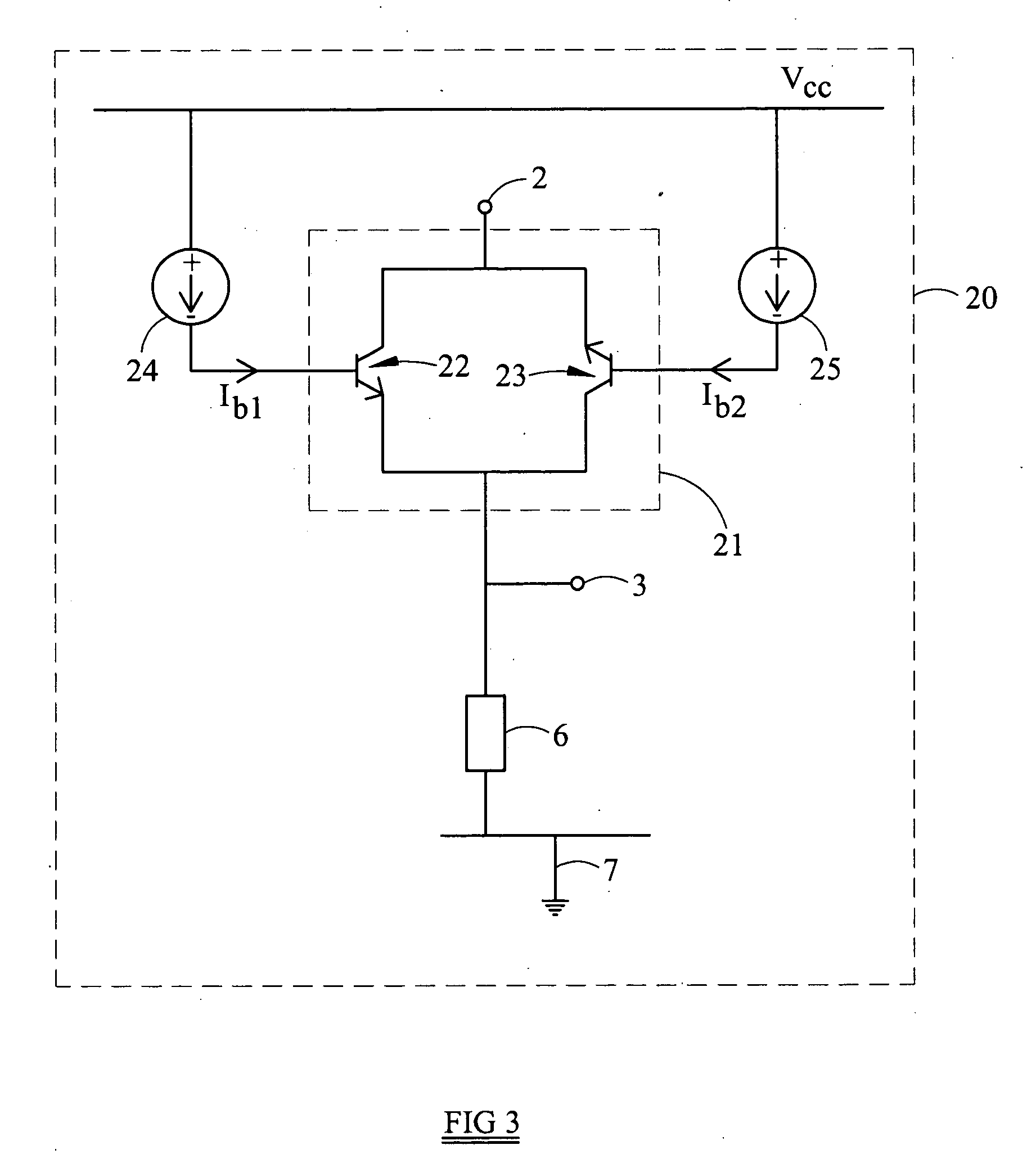
[0047] Referring now to FIG. 3 this illustrates an analogue switching circuit 20 in accordance with the present invention, which is a modification of the prior art analogue switching circuit of FIG. 1. Components common to the circuits of FIGS. 1 and 3 are identified by the same reference numerals. Switching circuit 20 comprises an analogue switch 21 in accordance with the present invention connected between the first and second switching terminals 2, 3. Switch 21 comprises a first bipolar transistor 22 having its collector connected to the first switch terminal 2 and its emitter connected to the second switch terminal 3. Switch 21 further comprises a second bipolar transistor 22 having its emitter connected to the first switch terminal 2 and its collector connected to the second switch terminal 3.

[0048] This back to back arrangement of transistors may be turned on, i.e. allowing current to pass between the switch terminals 2, 3 by applying control currents Ib1 and Ib2 to the bases ...

second embodiment

[0052] Referring now to FIG. 4, this illustrates a switching circuit comprising switching circuit 20 and a slave switching circuit 30 according to the present invention. Switching circuit 20 is identical to that shown in FIG. 3, except for the additional connections to slave switching circuit 30. The same reference numerals will be used to refer to components common to FIGS. 3 and 4.

[0053] Slave switching circuit 30 comprises a slave switch 31 connected between first and second slave terminals 32, 33. The slave switch 31 is a duplicate of the analogue switch 21, comprising third and fourth bipolar transistors 34, 35. Third transistor 34 has its collector connected to the first slave terminal 32 and its emitter connected to the second slave terminal 33. Fourth transistor 35 has its emitter connected to the first slave terminal 32 and its collector connected to the second slave terminal 33.

[0054] Third and fourth transistors 34, 35 are turned on by slave control currents Ib3 and Ib4 ...


PUM


Abstract

A switching circuit (20) comprising first and second switch terminals (2,3) and a switch (21). The switch (21) comprises a first bipolar transistor (22), having a collector connected to the first switch terminal (2) and an emitter connected to the second switch terminal (3), and a second bipolar transistor (23), having an emitter connected to the first switch terminal (2) and a collector connected to the second switch terminal (3). The switch (21) can be turned on by supply of a control current to the base of either the first or the second bipolar transistor.

Description

CROSS-REFERENCE TO RELATED PATENT APPLICATIONS [0001] Great Britain Priority Application 0421116.5, filed Sep. 23, 2004 including the specification, drawings, claims and abstract, is incorporated herein by reference in its entirety. SUMMARY OF THE INVENTION [0002] The present invention relates to an analogue switch. In particular, the invention relates to an analogue switch fabricated from bipolar transistors. [0003] In the design of analogue circuits, in particular analogue integrated circuits, there is commonly a requirement for an analogue switch. An analogue switch operates such that when the switch is closed a voltage at a first switch terminal, derived from other parts of the circuit, is switched to a second switch terminal. A load, which may be a single component or a further portion of the circuit, is connected to the second switch terminal. Therefore, when the switch is closed, current passes though the switch to the load. [0004] MOSFET transistors are commonly used as anal...

Claims


Application Information

Patent Timeline
Patent Type & Authority Applications(United States)
IPC IPC(8): H03K17/687
CPCH03K17/68H03K17/664
Inventor DODD, ALAN JAMESJENKINS, JOSEPH ANDREWSULLIVAN, ANTHONY PHILIP
Owner ZETEK
Why Eureka
Try Eureka