Apparatus and method for inspecting pattern

a pattern and pattern technology, applied in the field of pattern inspection techniques, can solve the problems of not meeting the required accuracy, not being able to easily perform a pattern inspection, and not being able to classify defects with high accuracy in some cases, and achieve the effect of high accuracy

Inactive Publication Date: 2006-03-30
DAINIPPON SCREEN MTG CO LTD
View PDF18 Cites 30 Cited by
  • Summary
  • Abstract
  • Description
  • Claims
  • Application Information

AI Technical Summary

Benefits of technology

[0010] The present invention is intended for an apparatus for inspecting pattern on an object. It is an object of the present invention to classify a class of a defect candidate of pattern on an object with high accuracy. It is another object of the present invention to perform a classification of a defect candidate easily.

Problems solved by technology

Recently, it is required to increase the accuracy of classification of defects, however, even if geometric feature values or feature values representing density are obtained as the methods disclosed in Documents 1 or 3, it is difficult to classify classes of defects with high accuracy in some cases.
In this case, even if the method based on leaning such as neural network in Document 3 is used, since the accuracy of classification largely depends on a type of inputted feature value in general, it is not possible to meet the required accuracy.
Thus, it is not possible to perform a classification of defects easily.

Method used


Image

  • Apparatus and method for inspecting pattern
  • Apparatus and method for inspecting pattern
  • Apparatus and method for inspecting pattern

Examples


Embodiment Construction

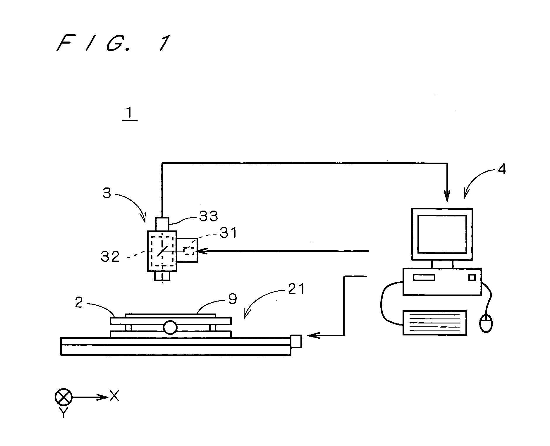
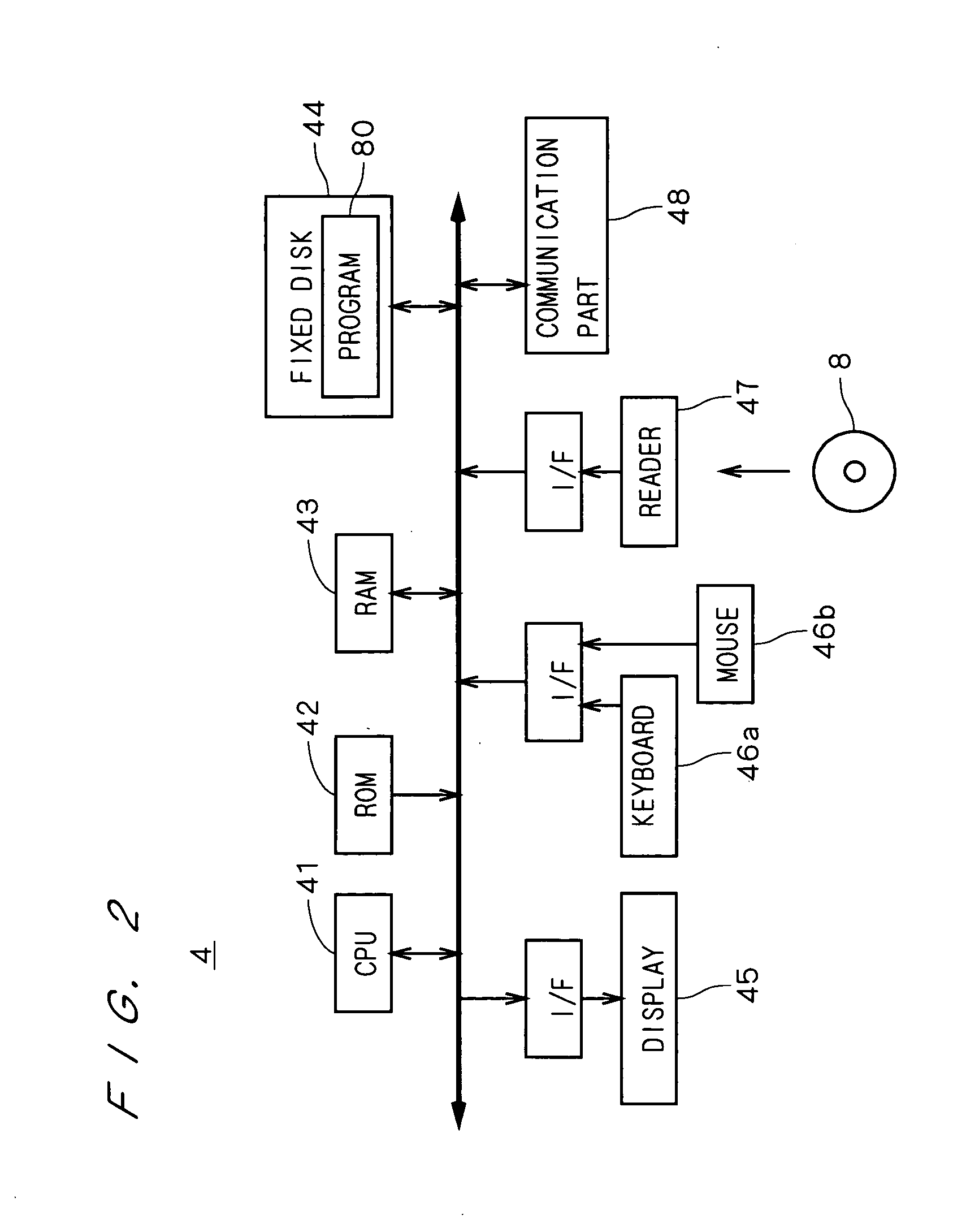
[0034]FIG. 1 is a view showing a construction of a pattern inspection apparatus 1 in 20 accordance with the first preferred embodiment of the present invention. The pattern inspection apparatus 1 comprises a stage 2 for holding a semiconductor substrate (hereinafter, referred to as a “substrate”) 9 formed predetermined wiring pattern, an image pickup part 3 for performing an image pickup of the substrate 9 to acquire a grayscale image of the substrate 9, a stage driving part 21 for moving the stage 2 relatively to the image pickup part 3 and a computer 4 constituted of a CPU which performs various computations and memories which store various information and the like. Each constituent element of the pattern inspection apparatus 1 is controlled by the computer 4.

[0035] The image pickup part 3 comprises a lighting part 31 for emitting an illumination light, an optical system 32 for guiding the illumination light to the substrate 9 and receiving the light from the substrate 9 and an i...


PUM


Abstract

An operation part (50) in a pattern inspection apparatus (1) comprises a defect candidate image generator (511) for generating a binary defect candidate image representing a defect candidate area in an inspection image by comparing the inspection image with a reference image, in an inspection image masking part (521) the inspection image is masked with the defect candidate image to obtain a masked inspection image. In a feature value calculation part (531), an autocorrelation feature value is obtained from the masked inspection image, and outputted to a classifying part (54). The classifying part (54) comprises a classifier (541) outputting a classification result on the basis of the autocorrelation feature value and a classifier construction part (542) for constructing the classifier (541) by learning. It is thereby possible to easily perform the high accurate classification of defect candidate using the autocorrelation feature value which is hard to characterize as compared with geometric feature value or feature value representing density.

Description

BACKGROUND OF THE INVENTION [0001] 1. Field of the Invention [0002] The present invention relates to a technique for inspecting pattern on an object. [0003] 2. Description of the Background Art [0004] A comparison check method has been mainly used, conventionally, in a field of inspection of pattern formed on a semiconductor substrate, a glass substrate, a printed circuit board or the like. For example, in binary image, an image of exclusive OR of an inspection image (an image to be inspected) and a reference image is obtained, and in grayscale image, an absolute difference value image which represents absolute values of the difference between pixel values in an inspection image and pixel values in a reference image is obtained and each pixel is binarized by a predetermined threshold value, to detect an area of a defect. [0005] In the circuit formation process or the like of a semiconductor substrate, a pattern inspection apparatus with a function to classify a class of a detected d...

Claims


Application Information

Patent Timeline
Patent Type & Authority Applications(United States)
IPC IPC(8): G06K9/00
CPCG06T2207/30148G06T7/001
Inventor ONISHI, HIROYUKIASAI, HIROSHIOGI, HIROSHI
Owner DAINIPPON SCREEN MTG CO LTD
Why Eureka
Try Eureka