Thin film circuit device, manufacturing method thereof, electro-optical apparatus, and electronic system

a thin film circuit and manufacturing method technology, applied in the direction of optics, identification means, instruments, etc., can solve the problem of not proposing the vertical connection of thin film circuits to each other, and achieve the effect of enhancing the lamination accuracy of thin film circuit layers and facilitating lamination

Inactive Publication Date: 2006-03-30
SEIKO EPSON CORP
View PDF6 Cites 13 Cited by
  • Summary
  • Abstract
  • Description
  • Claims
  • Application Information

AI Technical Summary

Benefits of technology

[0013] According to the structure described above, since the connection electrode is exposed outside, the thin film circuit layer and the exterior circuit can be connected to each other. Hence thin film circuit layers can be easily laminated to each other.
[0016] According to the structure described above, a basic thin film circuit layer can be obtained to form a thin film circuit laminate device which is composed of a plurality of said thin film circuit layers. When a peeling and transferring process is repeated using the structure described above, a laminate of the thin film circuit layers can be easily formed.
[0017] The thin film circuit device described above may further include a protective layer between the peeling layer and the underlayer. By the presence of this protective layer mentioned above, damage done to the thin film circuit layer in a peeling and transferring process, in particular, damage done to the connection electrode in contact with the peeling layer can be reduced or prevented.
[0021] The lower connection electrode may be formed approximately flush with the underlayer. Hence, the bottom surface of the thin film circuit layer is planarized, and as a result, the lamination can be easily performed.
[0022] The bottom surface of the first thin film circuit layer and that of the second thin film circuit layer may be formed approximately parallel to each other. Hence, the lamination accuracy of the thin film circuit layers can be enhanced.
[0028] The method to manufacture a thin film circuit device, described above, may include: forming a protective layer between the peeling layer and the thin film circuit layer; and removing the protective layer after the thin film circuit layer is peeled away to transfer. Accordingly, the damage done to the thin film circuit layer in a peeling and transferring process, in particular, the damage done to the connection electrode in contact with the peeling layer can be reduced or prevented.

Problems solved by technology

However, wire connection between thin film circuits laminated to each other in the vertical direction has not been proposed.

Method used


Image

  • Thin film circuit device, manufacturing method thereof, electro-optical apparatus, and electronic system
  • Thin film circuit device, manufacturing method thereof, electro-optical apparatus, and electronic system
  • Thin film circuit device, manufacturing method thereof, electro-optical apparatus, and electronic system

Examples


Embodiment Construction

[0039] Hereinafter, the exemplary embodiments of the present invention will be described with reference to drawings.

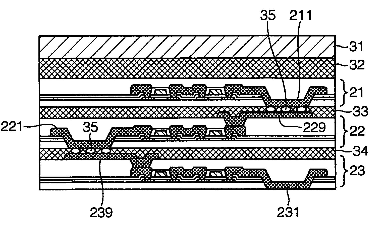
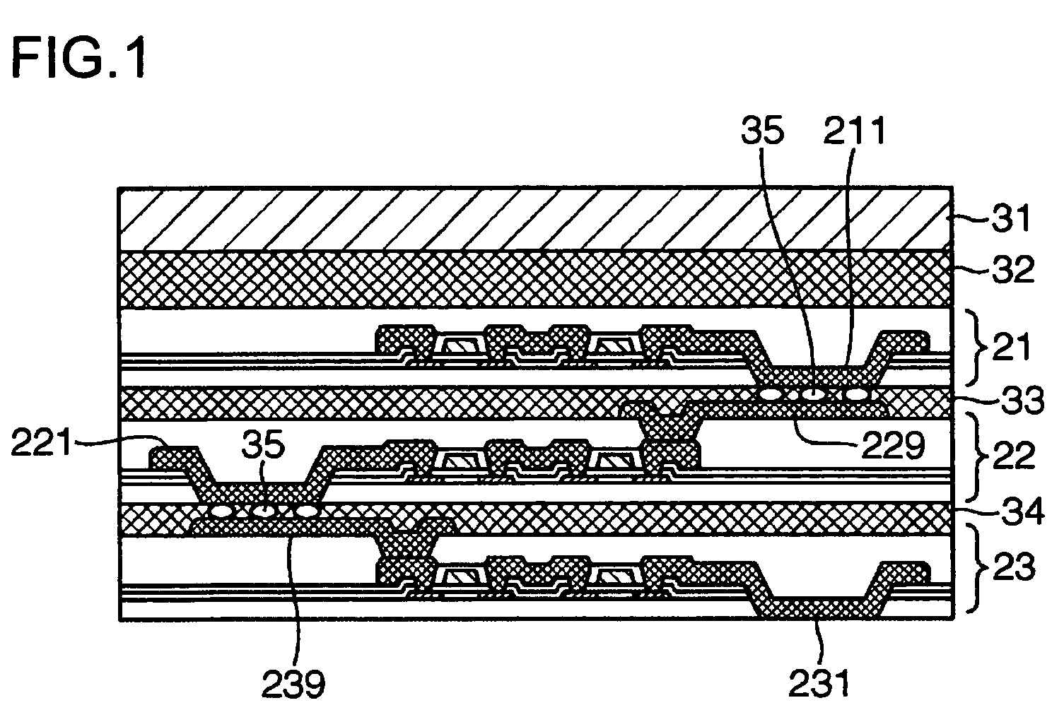
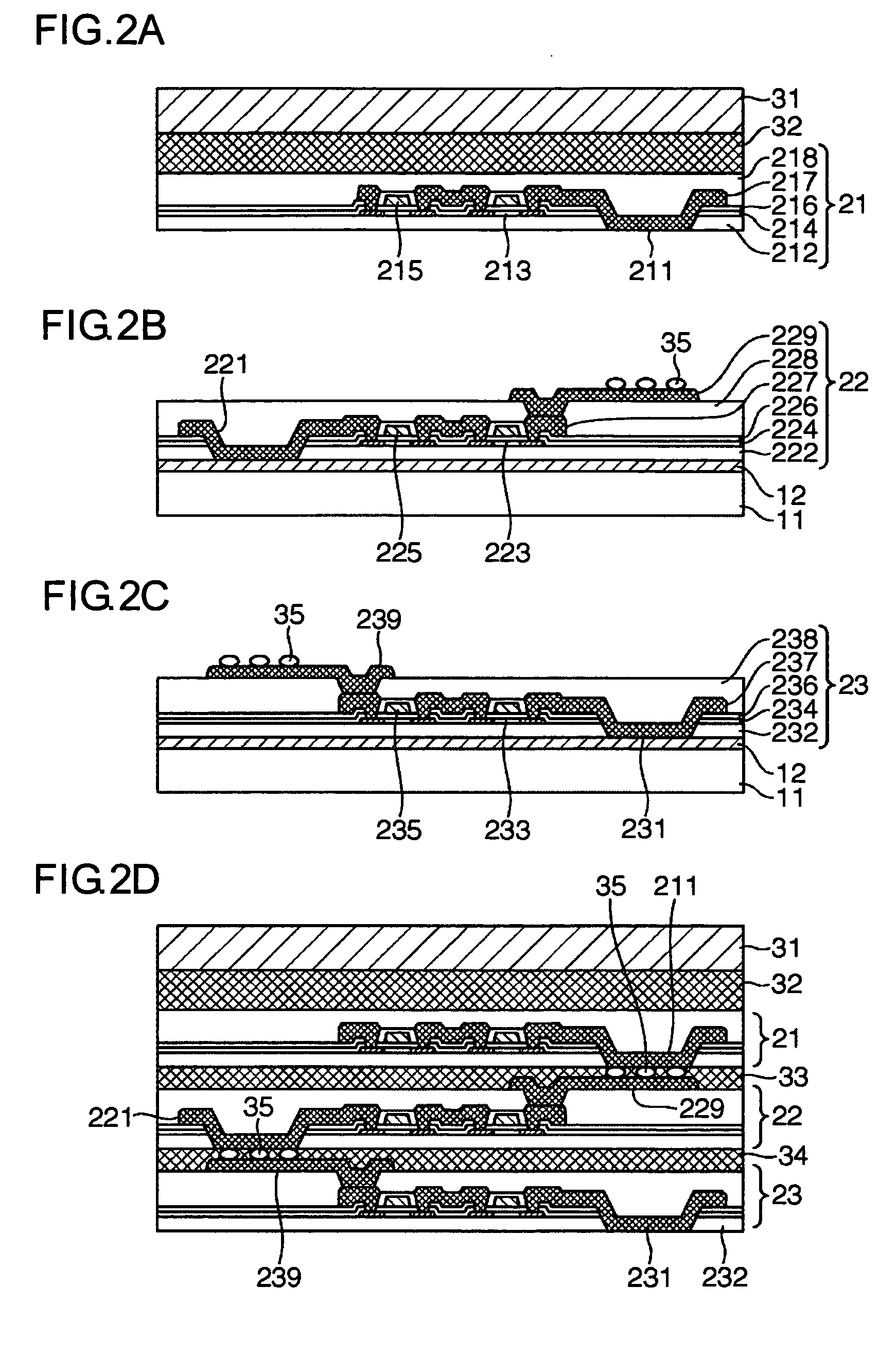
[0040] A thin film circuit device of an exemplary embodiment of the present invention has a structure in which thin film circuits are laminated to each other in the vertical direction, and in which, among the circuits mentioned above, an intermediate thin film circuit present inside the laminate is formed to have electrodes on the upper and the lower surfaces thereof for electrical connection. In addition, in the thin film circuit device according to the exemplary embodiment of the present invention, since an electrode is formed which is exposed at the rear surface of the thin film circuit, connection with a thin film circuit located thereunder and / or an exterior wire can be easily achieved.

[0041] In a manufacturing method according to an exemplary embodiment of the present invention, a process to manufacture a thin film circuit device using a peeling and transferrin...


PUM

PropertyMeasurementUnit
energyaaaaaaaaaa
temperatureaaaaaaaaaa
heat resistantaaaaaaaaaa

Abstract

To provide a thin film circuit device in which a three-dimensional circuit structure is realized, a thin film circuit device is formed of a first thin film circuit layer and a second thin film circuit layer laminated to each other. The first thin film circuit layer contains a first thin film circuit provided between an underlayer and a protective layer and a lower connection electrode connected to the first thin film circuit and exposed at a part of the bottom surface of the underlayer. The second thin film circuit layer contains a second thin film circuit provided between an underlayer and a protective layer, an upper connection electrode connected to the second thin film circuit and exposed at a part of the top surface of the protective layer, and a lower connection electrode connected to the second thin film circuit and exposed at a part of the bottom surface of the underlayer. The first and the second thin film circuits are bonded to each other so that the lower connection electrode of the first thin film circuit layer is electrically connected to the upper electrode of the second thin film circuit layer.

Description

[0001] This is a Division of application Ser. No. 10 / 850,405, filed May 21, 2004. The entire disclosure of the prior application is hereby incorporated by reference herein in its entirety.BACKGROUND OF THE INVENTION [0002] 1. Field of Invention [0003] The present invention relates to thin film circuit devices having a three-dimensional thin film circuit and to methods to manufacture a thin film circuit device having a three-dimensional circuit structure. [0004] 2. Description of Related Art [0005] In semiconductor devices and the like, since high temperature processes and the like are performed when necessary layers and regions are formed on a substrate to form a laminate, selection of members to form substrates and laminates may be restricted in some cases. For example, resin films, plastic substrates, and the like are not suitable in a high temperature process. [0006] Hence, for example, according to Japanese Unexamined Patent Application Publication No. 2002-217391, a peeling and...

Claims


Application Information

Patent Timeline
Patent Type & Authority Applications(United States)
IPC IPC(8): H01L21/84G02F1/1345G02F1/136G09F9/30H01L21/02H01L21/336H01L21/768H01L21/77H01L21/8238H01L23/52H01L27/00H01L27/08H01L27/092H01L27/12H01L29/786H01L51/50
CPCH01L27/1266H01L27/124H01L2221/68363H01L2224/32145H01L2224/83001G02F1/136
Inventor UTSUNOMIYA, SUMIO
Owner SEIKO EPSON CORP
Why Eureka
Try Eureka